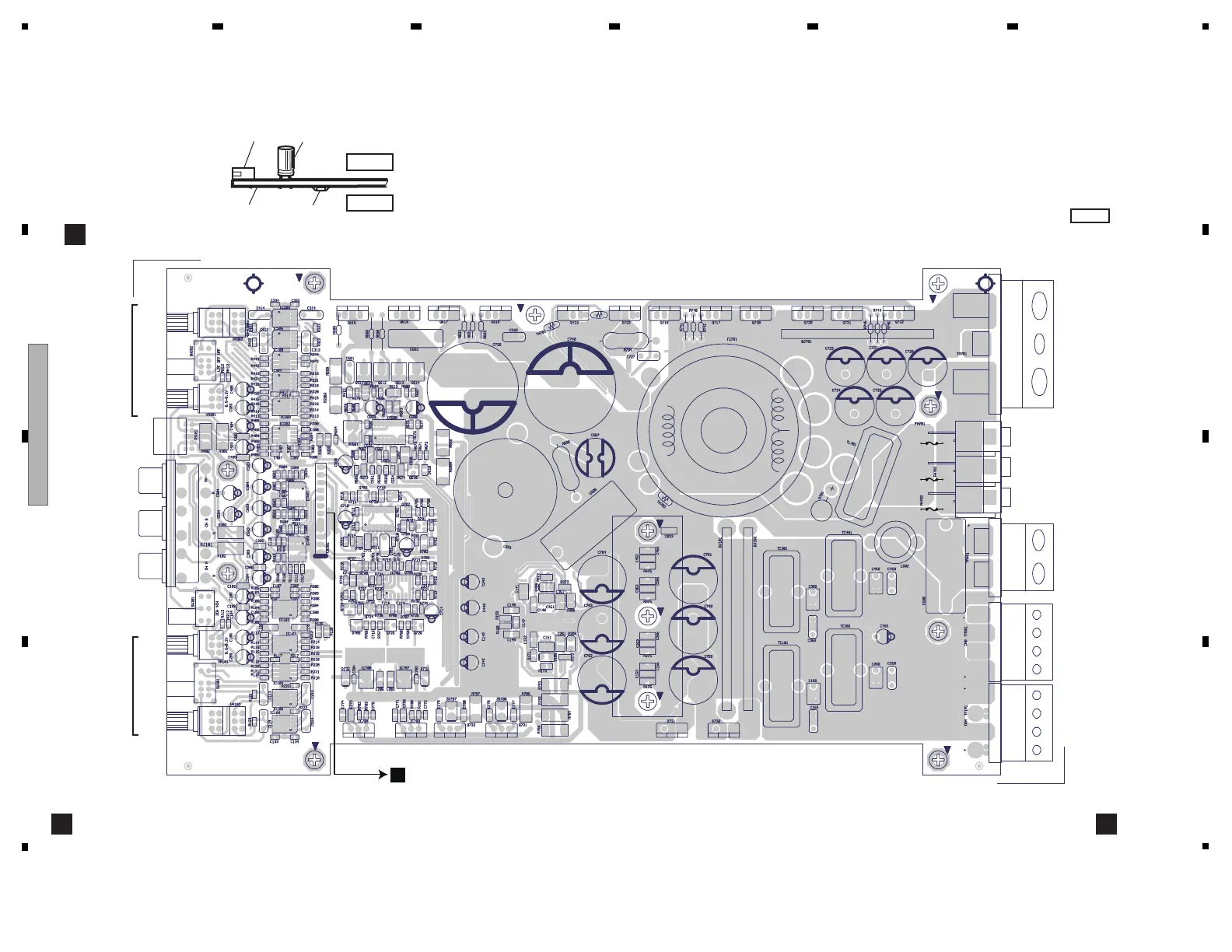
11. PCB CONNECTION DIAGRAM
AA
A
MAIN PCBA
SIDE A
Capacitor
Connector
P.C.Board
Chip Part
SIDE B
SIDE A
NOTE FOR PCB DIAGRAMS
1.The parts mounted on this PCB
include all necessary parts for
several destination.
For further information for
respective destinations, be sure
to check with the schematic dia-
gram.
2.Viewpoint of PCB diagrams
GND
FREQ
CH B
CH B INPUT
CH A INPUT
4CH
2CH
INPUT
SELECT
GAIN
FILTER
OUTPUT
S.CONTROL
POWER
SPEAKER
OUTPUT
BL+
AL+
AL-
AR-
AR+
BL-
BR-
BR+
>
>
>
FREQ
CH A
GAIN
FILTER
HFP
LFP
OFF
HFP
LFP
OFF
B
CN501
PCB CONNECTION DIAGRAM
 Loading...