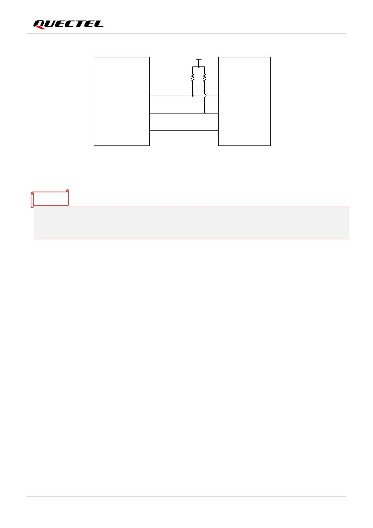
1. I2C_SDA/I2C_SCL should be externally pulled up to V
IO
= 2.8 V.
2. The I2C voltage threshold of L76-L module is 2.8 V. If the system voltage of MCU is not consistent
with it, a level shifter circuit must be used.
4.1.2. ANTON
The modules provide a pin called ANTON which is related to module state. Its voltage level will change in
different module states. When the modules work in Continuous mode, this pin is in high level. While the
modules work in Standby mode, GLP mode, Backup mode, AlwaysLocate™ mode, and during sleep time
in periodic mode, this pin is in low level. Based on this characteristic, the ANTON pin can be used to
control the power supply of active antenna or the ENABLE pin of the additional LNA to reduce power
consumption.
4.1.3. 1PPS
The 1PPS output generates one pulse per second trains synchronized with a GPS or UTC time grid with
intervals configurable over a wide range of frequencies. The accuracy is < 100 ns. Thus, it may be used
as a low frequency time synchronization pulse or as a high frequency reference signal.
The latency range is 465-485 ms between the beginning of UART TXD and the rising edge of PPS.
 Loading...