GNSS Module Series
L76&L76-L_Hardware_Design 41 / 59
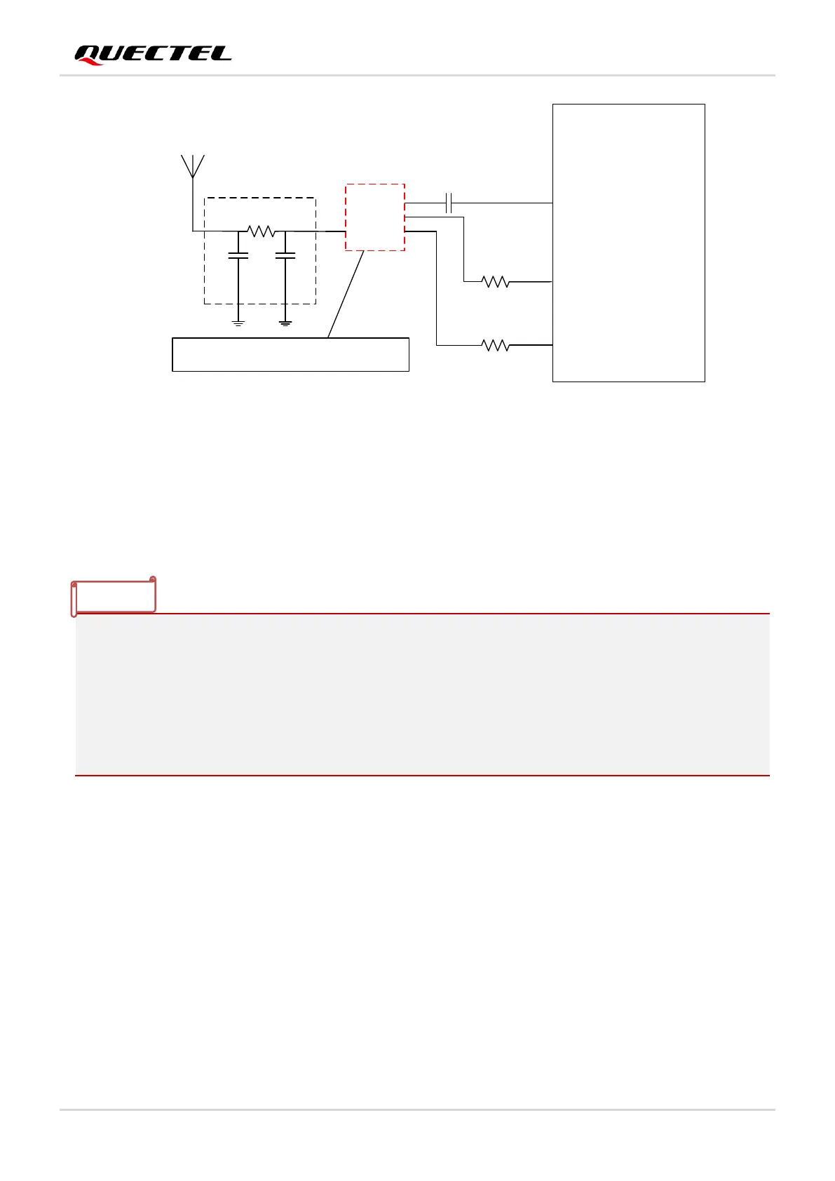
Module
VDD_RF
Passive Antenna
R3
RF_IN
C1 NM
π Matching Circuit
LNA
RF IN
VCC
ENABLE
RF OUT
R1
C2 NM
C3 56 pF
100R
ANTON
R2
100R
0R
No need to add for L76-L And L76-L(L)
which has an embedded LNA
Figure 22: Reference Design for Passive Antenna with Additional LNA
C1, R1, C2 form a reserved matching circuit for passive antenna and LNA. By default, C1 and C2 are not
mounted; R1 is 0 Ω. C3 is reserved for impedance matching between LNA and the module and the default
value of C3 capacitor is 56 pF which you might optimize according to the real conditions. ANTON is an
optional pin which can be used to control the ENABLE pin of an additional LNA.
1. There is no need to use an additional LNA for L76-L and L76-L(L) modules, because there is
already an embedded LNA inside these two modules.
2. The selected LNA should support both GPS and GLONASS system. For more information, please
contact Quectel technical supports.
3. The power consumption of the device can be reduced by controlling the LNA ENABLE pin through
the ANTON pin of the modules. If ANTON function is not used, please connect the LNA ENABLE
pin to VCC and keep LNA always on.
5.3. Coexistence with Cellular Systems
Since GNSS signals are usually very weak, a GNSS receiver could be vulnerable to the interference of
the surrounding environment. According to 3GPP specifications, a cellular terminal should transmit a
signal of up to 33 dBm at GSM bands, or of about 24 dBm at WCDMA and LTE bands. As a result,
coexistence with cellular systems must be optimized to avoid significant deterioration of the GNSS
performance.
 Loading...