M12 Hardware Design
M12_Hardware_Design_V3.3 - 61 -
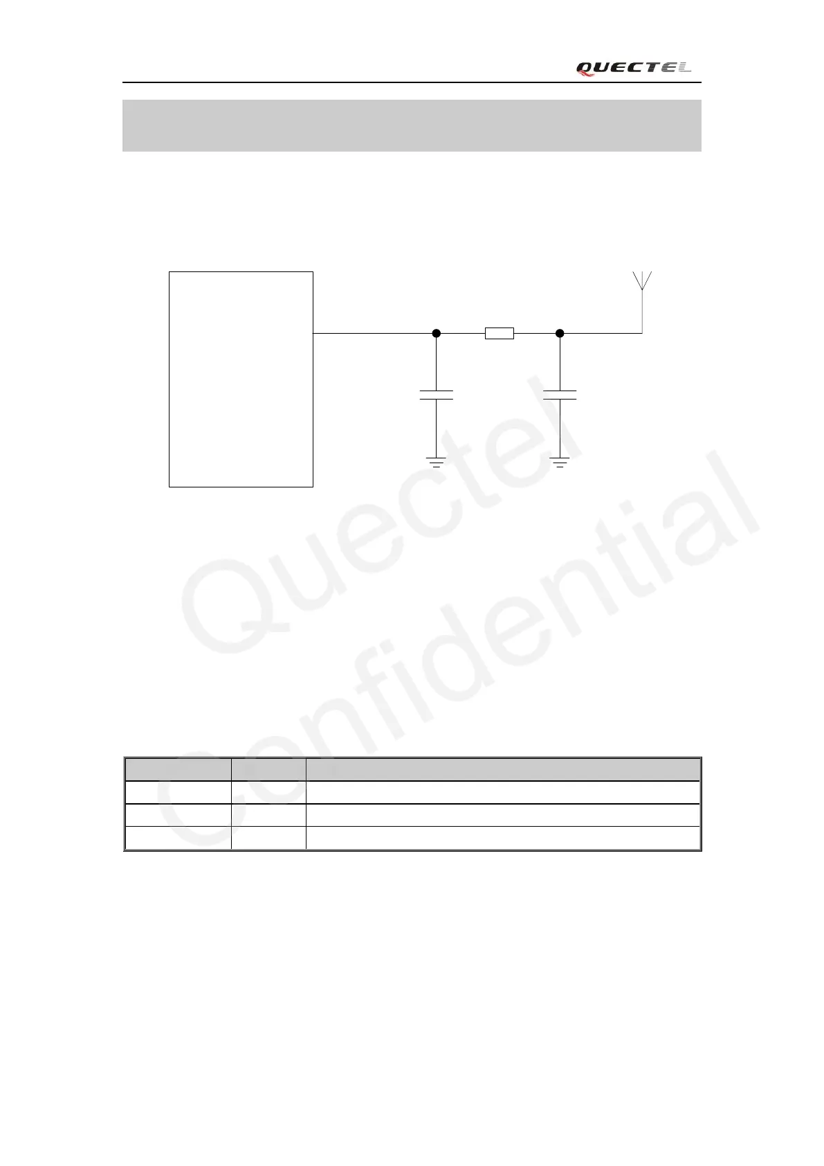
4. Antenna interface
The Pin 43 is the RF antenna pad. The RF interface has an impedance of 50Ω. A reference circuit
is shown in the following figure. In order to adjust RF performance, it should reserve a П-type
matching circuit. By default, the resistance of R1 is 0Ω and capacitors C1 and C2 are not soldered.
RF_ANT
R1 0R
C1
NM
C2
NM
Module
Figure 44: Reference circuit of RF interface
4.1. Antenna installation
M12 provides an RF antenna PAD for customer’s antenna connection. The RF trace in host PCB
connected to the module’s RF antenna pad should be coplanar waveguide line or microstrip line,
which characteristic impedance should be close to 50Ω. M12 comes with two grounding pads
which are next to the antenna pad in order to give a better grounding.
Table 24: Pin definition of the RF_ANT
To minimize the loss on the RF trace and RF cable, they should be designed carefully. It is
recommended that the insertion loss should try to meet the following requirements:
EGSM900<1dB
DCS1800 <1.5dB
 Loading...