GSM/GPRS Module Series
M35 User Manual
M35_User_Manual Confidential / Released 26 / 85
VBAT
C2C1
+
C3 C4
GND
100uF 100nF 10pF
0603
33pF
0603
Figure 4: Reference Circuit for the VBAT Input
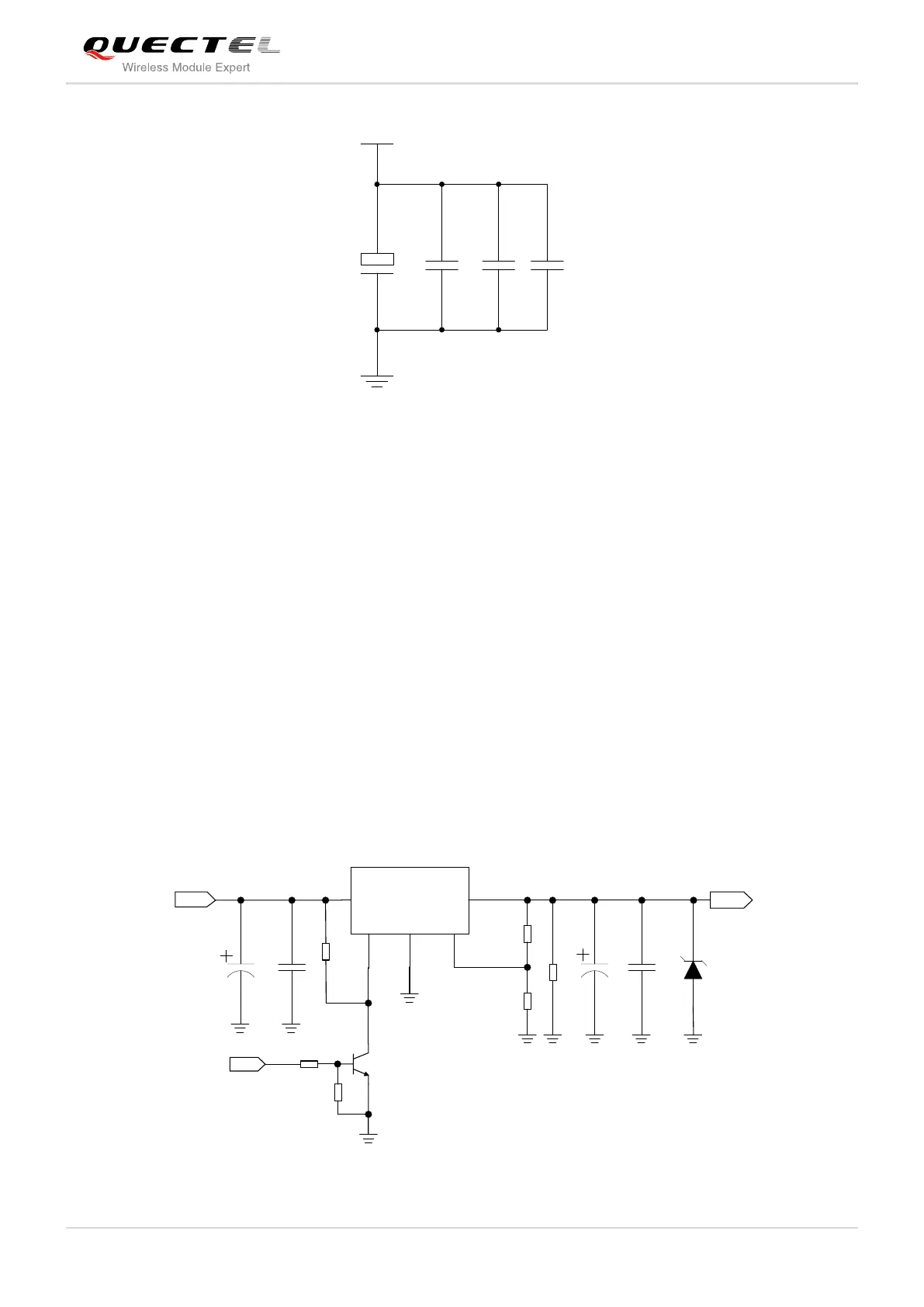
3.3.3. Reference Design for Power Supply
The power design for the module is very important, since the performance of power supply for the module
largely depends on the power source. The power supply is capable of providing the sufficient current up to
2A at least. If the voltage drop between the input and output is not too high, it is suggested to use a LDO
as module’s power supply. If there is a big voltage difference between the input source and the desired
output (VBAT), a switcher power converter is recommended to be used as a power supply.
Figure 5 shows a reference design for +5V input power source. The designed output for the power supply
is 4.0V and the maximum load current is 3A. In addition, in order to get a stable output voltage, a zener
diode is placed close to the pins of VBAT. As to the zener diode, it is suggested to use a zener diode of
which reverse zener voltage is 5.1V and dissipation power is more than 1 Watt.
DC_IN
C1
C2
MIC29302WU U1
IN OUT
EN
GND
ADJ
2 4
1
3
5
VBAT
100nF
C3
470uF
C4
100nF
R2
D1
124K
56K
R3
470uF
5.1V
R4
470R
MCU_POWER_ON/OFF
47K
4.7K
R5
R6
R1
51K
Figure 5: Reference Circuit for Power Supply

 Loading...