GSM/GPRS Module Series
M35 User Manual
M35_User_Manual Confidential / Released 43 / 85
The reference design for Debug Port is shown as below.
Peripheral
TXD
RXD
GND
Module
DBG_TXD
DBG_RXD
GND
Figure 21: Reference Design for Debug Port
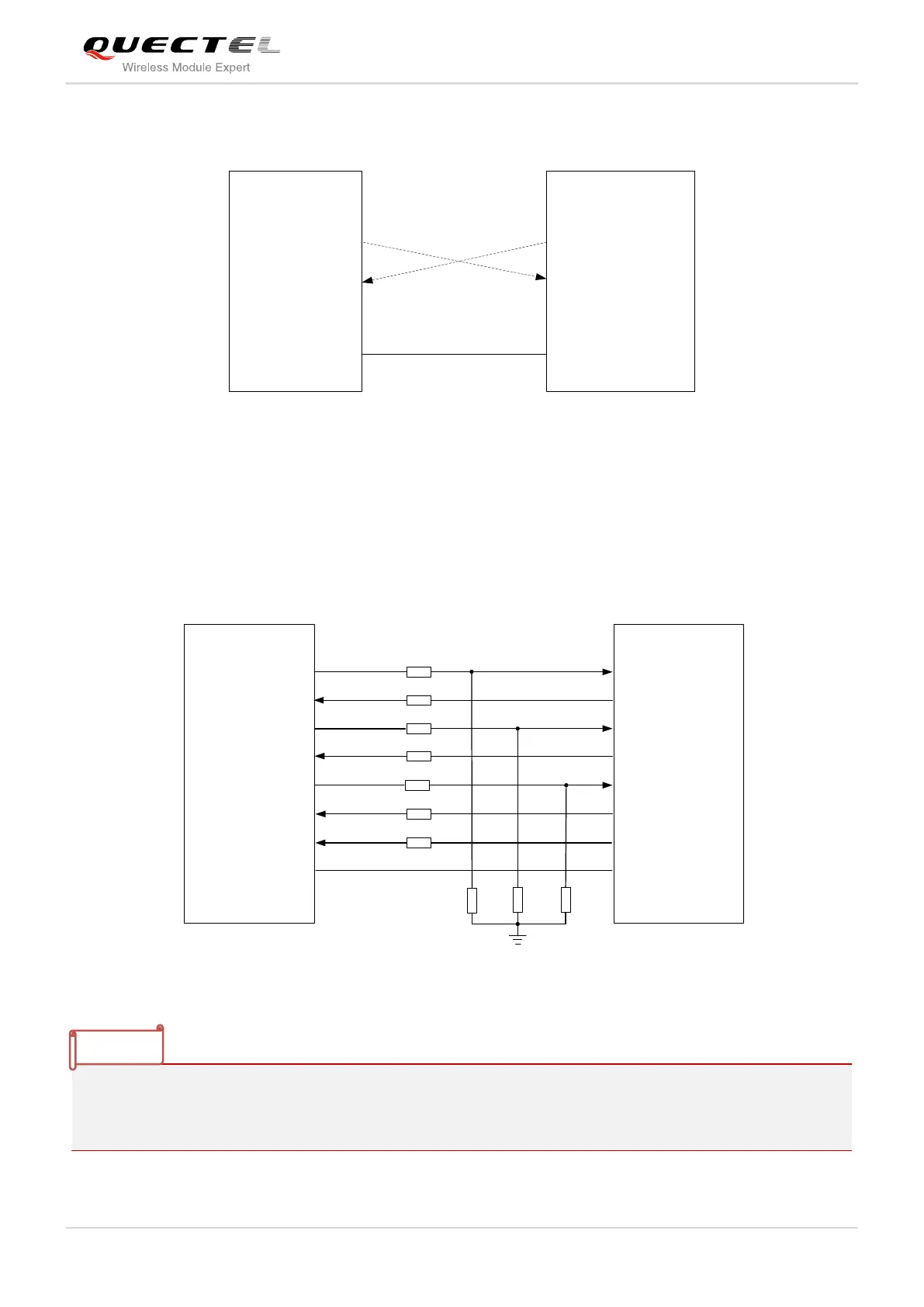
3.7.3. UART Application
The reference design of 3.3V level match is shown as below. If the host is a 3V system, please change
the 5.6K resistor to 10K.
Peripheral
/TXD
/RXD
1K
TXD
RXD
RTS
CTS
DTR
RI
/RTS
/CTS
GPIO
EINT
GPIO DCD
Module
1K
1K
Voltage level:3.3V
5.6K
5.6K
5.6K
1K
1K
1K
1K
GND GND
Figure 22: Level Match Design for 3.3V System
It is highly recommended to add the resistor divider circuit on the UART signal lines when the host’s level
is 3V or 3.3V. For the higher voltage level system, a level shifter IC could be used between the host and
the module. For more details about UART circuit design, please refer to document [8].

 Loading...