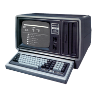
63
4.2 Model 4 FDC PCB #8858160
The TRS-80 Model III/4 Floppy Disk Interface Board
is an optional board which, if incorporated, provides a
standard 5-1/4” floppy disk controller. The Floppy
Disk Interface Board supports both single and double
density encoding schemes. Write precompensation
can be software enabled or disabled beginning at any
track, although the system software enables write
precompensation for all tracks greater than twenty-
one. The amount of write precompensation provided
is 250 nsec and is not adjustable. The data clock
recovery logic incorporates a digital data separator
which achieves state-of-the-art reliability. One to four
drives may be controlled by the interface (two internal
drives and two external). All data transfers are
accomplished by CPU data requests. In double
density operation, data transfers are synchronized to
the CPU by forcing a wait to the CPU and clearing
the wait by a data request from the FDC chip. The
end of the data transfer is indicated by generation of
a non-maskable interrupt from the interrupt request
output of the FDC chip. A hardware watchdog timer
insures that any error condition will not hang the wait
line to the CPU for a period long enough to destroy
RAM contents.
4.2.1 Control and Data Buffering
Refer to Schematic Diagram 8000168
The Floppy Disk Controller Board is an I/O port
mapped device which utilizes ports E4H, F0H, F1H,
F2H, F3H, and F4H. The decoding logic is
implemented on the CPU board. (Refer to Paragraph
3.1.4 Decoding Logic of the CPU operation). U4 is a
non-inverting octal buffer which isolates and buffers
the required control signals from the CPU board to
the FDC board. U2 is a bi-directional, 8-bit trans-
ceiver used to buffer data to and from the FDC board.
The direction of data transfer is controlled by the
combination of control signals DISKIN* and
RDNMISTATUS*. If either signal is active (logic low),
U2 is enabled to drive data onto the CPU board data
bus. If both signals are inactive (logic high), U2 is
enabled to receive data from the CPU board data
bus.
4.2.2 Nonmaskable Interrupt Logic
A dual D flip-flop (U12) is used to latch data bits D6
and D7 on the rising edge of the control signal
WRNMIMASKREG*. The outputs of U12 enable the
conditions which will generate a non-maskable
interrupt to the CPU. The NMI interrupt conditions are
programmed by doing an OUT instruction to port E4H
with the appropriate bits set. If data bit 7 is set, an
FDC interrupt request is enabled to generate an NMI
interrupt. If data bit 7 is reset, interrupt requests from
the FDC are disabled. If data bit 6 is set, a Motor
Time Out is enabled to generate a NMI interrupt. If
data bit 6 is reset, interrupts on Motor Time Out are
disabled. An IN instruction from port E4H enables the
CPU to check the FDC board to determine the source
of the non-maskable interrupt. Data bit 7 indicates the
status of FDC interrupt request (0 = true, 1 = false).
Data bit 6 indicates the status of Motor Time Out (0
true, 1 false). Data bit 5 indicates the status of the
Reset signal from the CPU board (0 = true, 1 = false).
The control signal RDNMISTATUS* gates this status
onto the CPU data bus when active (logic low).
4.2.3 Drive Select Latch and Motor ON Logic
Selecting a drive prior to a disk I/O operation is
accomplished by doing an OUT instruction to port
F4H with the proper bit set. The following table
described the bit allocation of the Drive Select Latch:
Data Bit Function
D0 Selects Drive 0 when set*
D1 Selects Drive 1 when set*
D2 Selects Drive 2 when set*
D3 Selects Drive 3 when set*
D4 Selects Side 0 when reset Selects
Side 1 when set
D5 Write precompensation enabled
when set, disabled when reset
D6 Generates WAIT if set
D7 Selects MFM mode if set Selects FM
mode if reset
*Only one of these bits should be set per output
A hex D flip-flop (U5) latches the drive select bits,
side select and FM*/MFM bits on the rising edge of
the control signal IDRVSEL*. A dual D flip-flop (U15)
is used to latch the Wait Enable and Write
precompensation enable bits on the rising edge of
IDRVSEL*. The rising edge of IDRVSEL* also
triggers a one-shot (1/2 of U13) which produces a
Motor On to the disk drives. The duration of the Motor
On signal is approximately two seconds. The spindle
motors are not designed for continuous operation,
therefore the inactive state of the Motor On signal is
used to clear the Drive Select Latch, which de-selects
any drives which were previously selected. The Motor
On one-shot is retriggerable by simply executing
another OUT instruction to the Drive Select Latch.
4.2.4 Wait State Generation and WAITIMOUT
Logic
As previously mentioned, a wait state to the CPU can
be initiated by an OUT to the Drive Select Latch with
D6 set. Pin 5 of U1 5 will go high after this operation.
This signal is inverted by 1/6 of U1 and is routed to
the CPU board where it forces the Z-80 into a wait
state. The Z-80 will remain in the wait state as long
as WAIT* is low. Once initiated, the WAIT* will
remain low until one of four conditions is satisfied.
One half of U9 (a five input NOR gate) is used to
 Loading...