RL78/G13 Clock Generator (Clock Switching) CC-RL
R01AN2831EJ0100 Rev. 1.00 Page 7 of 51
May 28, 2015
4. Description of the Hardware
4.1 Hardware Configuration Example
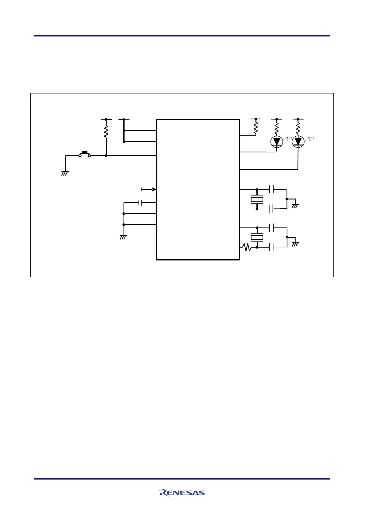
Figure 4.1 shows an example of hardware configuration that is used for this application note.
Figure 4.1 Hardware Configuration
Cautions: 1. The purpose of this circuit is only to provide the connection outline and the circuit is simplified
accordingly. When designing and implementing an actual circuit, provide proper pin treatment and make
sure that the hardware's electrical specifications are met (connect the input-only ports separately to V
DD
or V
SS
via a resistor).
2. Connect any pins whose name begins with EV
SS
to V
SS
and any pins whose name begins with EV
DD
to
V
DD
, respectively.
3. V
DD
must be held at not lower than the reset release voltage (V
LVD
) that is specified as LVD.
4. The LED connected to P63 is always off.
RESET
EV
DD
V
DD
EV
ss
V
ss
REGC
P137/INTP0
P40/TOOL0
P62
XT1
XT2
32.768 kHz
X1
X2
20 MHz
10 k
V
DD
P63
EV
DD
RL78/G13
EV
DD
For on-chip debu
er
V
DD
V
DD

 Loading...


