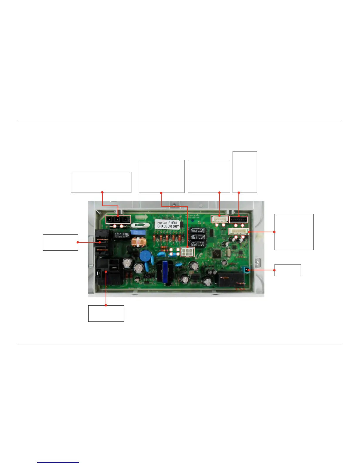
72 _ PCB Diagram
6-2. DETAILED DESCRIPTIONS OF CONTACT TERMINALS (MAIN PCB)
► RY7
1. Heater1RelaySwitch
2. Heater1RelaySwitch
► RY5
1. MotorRelaySwitch
2. MotorRelaySwitch
► CN6
1. SET GND
► CN1
1. ACPowerPort
2. ACPoweroffDetectionSensor
3. Door Detection Sensor(LOCK,UNLOCK)
► CN5(SteamModelsOnly)
1. STEAMVALVE1
2. Empty Pin
3. LAMP
4. Empty Pin
5. STEAMVALVE2
6. Empty Pin
► CN2
1. CommunicationsPort(Rx)
2. CommunicationsPort(Tx)
3. SUB RESET
4. 5V
5. DGND
6. 12V
► CN3
1. 5V
2. SO
3. SI
4. RESET
5. CLOCK
6. FLMDO
7. DGND
8. Empty Pin
1 3
g
4 6
g
3 1
g
6 1
g
8 1
g
7 1
g
► CN4
1. DGND
2. 5V
3. TEMP Sensor1
4. FabricDetectionSensor
5. FabricDetectionSensor
6. 5V
7. TEMP Sensor2
 Loading...