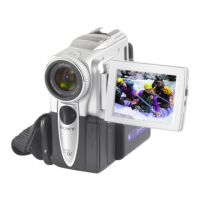
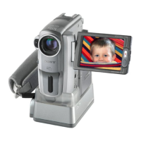
DCR-PC1000/PC1000E
4-77
4-3. PRINTED WIRING BOARDS
4-3. PRINTED WIRING BOARDS
board name
CD-569
CK-149
FP-164
FP-165
FP-166
FP-167
FP-168
FP-170
FP-172
FP-220
FP-236
FR-229
JK-285
PD-252
VJ-001
VC-398
parts location
(shown on page)
4-99
–
–
–
–
–
–
–
–
–
–
–
4-99
4-99
4-99
4 - 100, 101
number of layers
6
2
2
1
1
2
1
1
2
1
1
2
2
2
2
8
layers not shown
2 to 5
–
–
–
–
–
–
–
–
–
–
–
–
–
–
2 to 7
pattern
BOARD INFORMATION
waveforms
(shown on page)
4-97
–
–
–
–
–
–
–
–
–
–
–
–
4-97
–
4-98
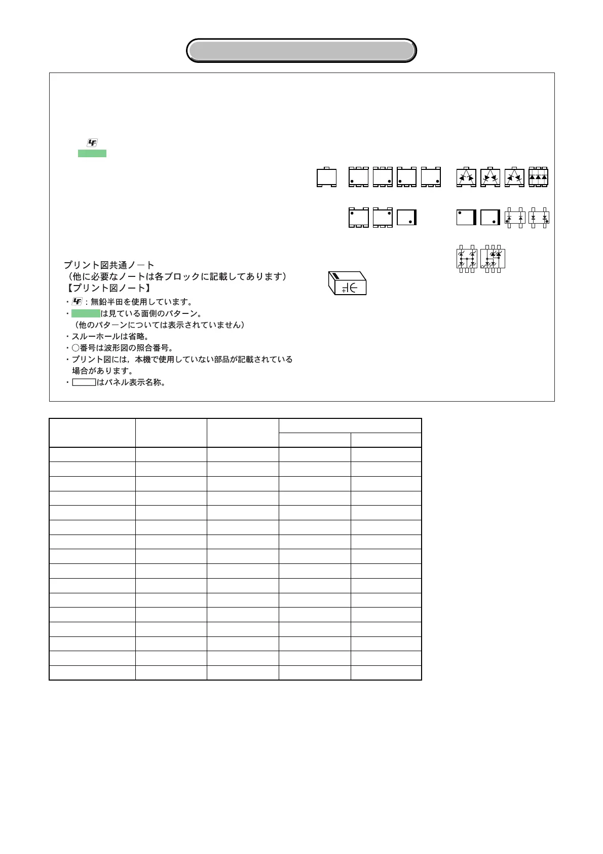
(For printed wiring boards)
•
: Uses unleaded solder.
•
: Pattern from the side which enables seeing.
(The other layers’ patterns are not indicated)
• Through hole is omitted.
• Circled numbers refer to waveforms.
• There are a few cases that the part printed on diagram
isn’t mounted in this model.
• C: panel designation
(ENGLISH)
THIS NOTE IS COMMON FOR WIRING BOARDS
(In addition to this, the necessary note is printed in each block)
21
3
21
3
21
3
345
21
123
654
EB
C
31
5
5
2
46
123
54
43
12
5
4
1
3
12
43
312
45
534
12
34
21
12
43
46
2
5
31
12
4
3
64
1
3
• Chip
• Capacitor
parts
Transistor Diode
(JAPANESE)
 Loading...