4-47
DSC-F828
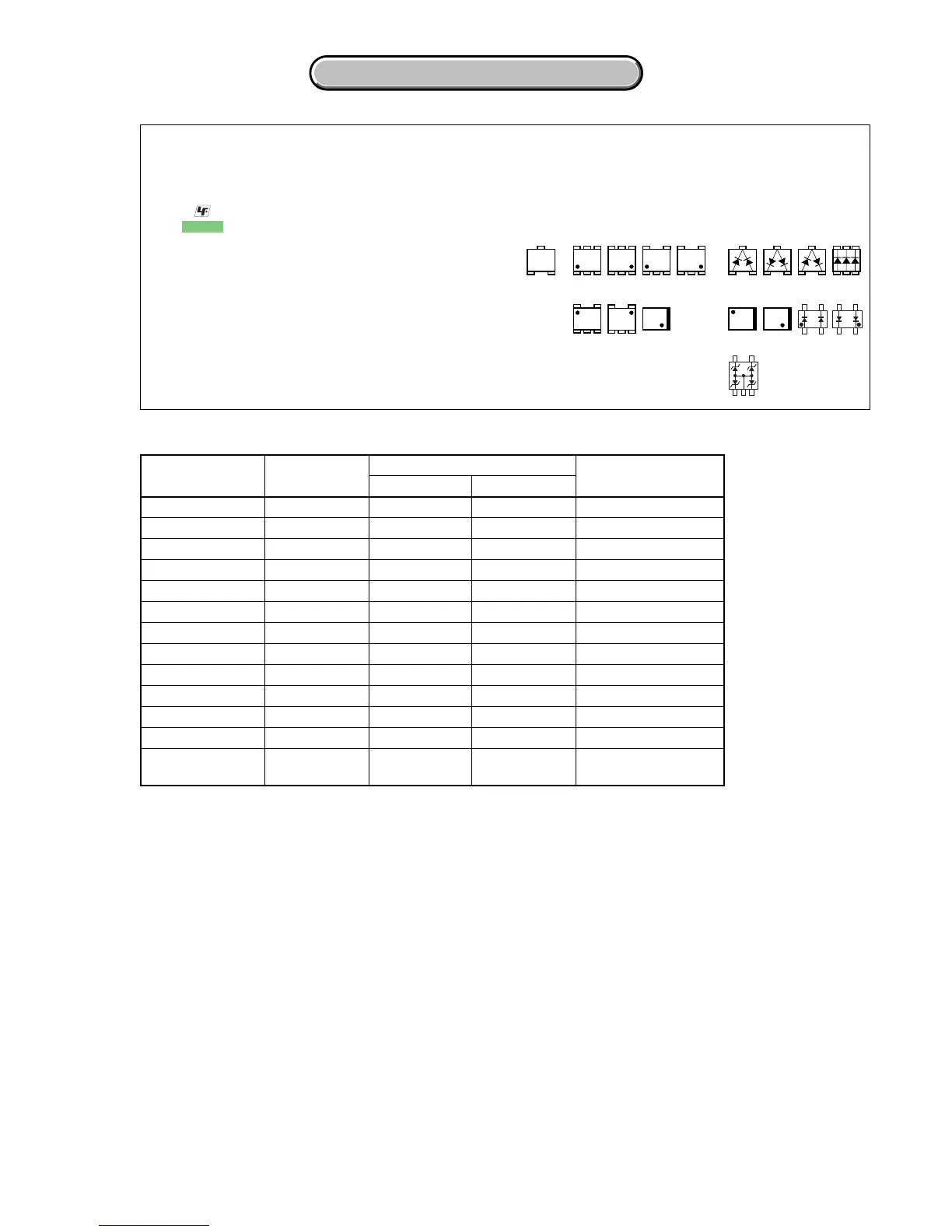
4-3. PRINTED WIRING BOARDS
4-3. PRINTED WIRING BOARDS
(For printed wiring boards)
•
: Uses unleaded solder.
• : Pattern from the side which enables seeing.
(The other layers’ patterns are not indicated)
• Through hole is omitted.
• Circled numbers refer to waveforms.
• There are a few cases that the part printed on diagram
isn’t mounted in this model.
• C: panel designation
THIS NOTE IS COMMON FOR WIRING BOARDS
(In addition to this, the necessary note is printed in each block)
21
3
21
3
21
3
345
21
123
654
EB
C
31
5
5
2
46
123
54
43
12
5
4
13
12
43
312
45
534
12
34
21
12
43
46
2
5
31
12
4
3
• Chip parts.
Transistor Diode
board name
DD-204
LR-018
ST-088
MT-067
LS-067
SI-037
LB-091
UA-003
CF-097
AJ-007
SW-410
FP-748
SY-096
parts location
(shown on page)
4-63
–
4-63
–
–
–
–
4-63
4-63
4-63
4-63
–
4-65
number of layers
6
1
6
1
1
1
1
1
2
2
2
1
8
layers not shown
2 to 5
–
2 to 5
–
–
–
–
–
–
–
–
–
2 to 7
CSP IC
–
–
–
–
–
–
–
–
–
–
–
–
IC301, 302, 401, 452,
501, 601
pattern
BOARD INFORMATION
 Loading...