2
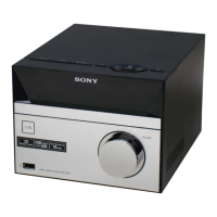
HCD-SPZ50/SPZ70
Notes on chip component replacement
• Never reuse a disconnected chip component.
• Notice that the minus side of a tantalum capacitor may be
damaged by heat.
Flexible Circuit Board Repairing
• Keep the temperature of the soldering iron around 270 ˚C
during repairing.
• Do not touch the soldering iron on the same conductor of the
circuit board (within 3 times).
• Be careful not to apply force on the conductor when soldering
or unsoldering.
TABLE OF CONTENTS
1. SERVICING NOTES ............................................... 3
2. GENERAL ................................................................... 5
3. DISASSEMBLY
3-1. Disassembly Flow ........................................................... 7
3-2. Case ................................................................................. 7
3-3. Front Panel Assy.............................................................. 8
3-4. Tape Mechaism Deck (CFP42601) ................................. 8
3-5. MAIN Board.................................................................... 9
3-6. Base Unit (BU-K6BD83S-WOD Assy)/
Belt (DLMA) ................................................................... 9
3-7. AMP/SP/POWER Board ................................................. 10
3-8. Tuner (FM/AM)............................................................... 10
4. TEST MODE.............................................................. 11
5. MECHANICAL ADJUSTMENT .......................... 13
6. ELECTRICAL ADJUSTMENT ............................ 13
7. DIAGRAMS
7-1. Block Diagram – CD SERVO Section – ......................... 15
7-2. Block Diagram – MAIN Section –.................................. 16
7-3. Block Diagram – AMP Section – .................................... 17
7-4. Block Diagram
– PANEL/POWER SUPPLY Section – ........................... 18
7-5. Printed Wiring Board – CD Board – ............................... 20
7-6. Schematic Diagram – CD Board – .................................. 21
7-7. Printed Wiring Board – TC Board – ................................ 22
7-8. Schematic Diagram – TC Board – .................................. 23
7-9. Printed Wiring Board – MAIN Board – .......................... 24
7-10. Schematic Diagram – MAIN Board (1/3) – .................... 25
7-11. Schematic Diagram – MAIN Board (2/3) – .................... 26
7-12. Schematic Diagram – MAIN Board (3/3) – .................... 27
7-13. Printed Wiring Board – AMP Board (SPZ50) – .............. 28
7-14. Schematic Diagram – AMP Board (SPZ50) –................. 29
7-15. Printed Wiring Board – AMP Board (SPZ70) – .............. 30
7-16. Schematic Diagram – AMP Board (SPZ70) –................. 31
7-17. Printed Wiring Board – PANEL Section (1/2) – ............. 32
7-18. Printed Wiring Boards – PANEL Section (2/2) –............ 33
7-19. Schematic Diagram – PANEL Section (1/2) – ................ 34
7-20. Schematic Diagram – PANEL Section (2/2) – ................ 35
7-21. Schematic Diagram – POWER Board –.......................... 36
7-22. Printed Wiring Board – POWER Board – ....................... 37
8. EXPLODED VIEWS
8-1. Overall Section ................................................................ 53
8-2. Front Panel Section ......................................................... 54
8-3. FL Section ....................................................................... 55
8-4. CD Section ...................................................................... 56
8-5. Power Section .................................................................. 57
9. ELECTRICAL PARTS LIST................................ 58
CAUTION
Use of controls or adjustments or performance of procedures
other than those specified herein may result in hazardous radiation
exposure.
SAFETY-RELATED COMPONENT WARNING!!
COMPONENTS IDENTIFIED BY MARK 0 OR DOTTED LINE
WITH MARK 0 ON THE SCHEMATIC DIAGRAMS AND IN
THE PARTS LIST ARE CRITICAL TO SAFE OPERATION.
REPLACE THESE COMPONENTS WITH SONY PARTS WHOSE
PART NUMBERS APPEAR AS SHOWN IN THIS MANUAL OR
IN SUPPLEMENTS PUBLISHED BY SONY.
4HISAPPLIANCEIS
CLASSIlEDASA#,!33
,!3%2PRODUCT4HIS
MARKINGISLOCATEDONTHE
REAREXTERIOR
General
Power requirements
Mexican model: 127 V AC, 60 Hz
Latin American model except for Mexican and Argentine models:
120 – 127 V or 220 – 240 V AC, 50/60 Hz
Adjustable with voltage selector
Other models: 220 – 240 V AC, 50/60 Hz
Power consumption:
HCD-SPZ70: 45 watts
HCD-SPZ50: 40 watts
Mass (excl. speakers): Approx. 4.1 kg
Design and specifications are subject to change without notice.
Ver. 1.3
Note: Refer to SUPPLEMENT-1 for the HP A-IN and MAIN boards
of printed wiring boards, schematic diagrams and electri-
cal parts list of HCD-SPZ70 Korean model.
w
w
w
.
x
i
a
o
y
u
1
6
3
.
c
o
m
Q
Q
3
7
6
3
1
5
1
5
0
9
9
2
8
9
4
2
9
8
T
E
L
1
3
9
4
2
2
9
6
5
1
3
9
9
2
8
9
4
2
9
8
0
5
1
5
1
3
6
7
3
Q
Q
TEL 13942296513 QQ 376315150 892498299
TEL 13942296513 QQ 376315150 892498299
http://www.xiaoyu163.com
http://www.xiaoyu163.com

 Loading...