— 7 —
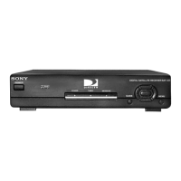
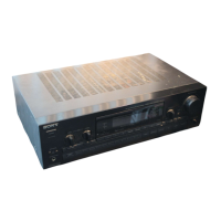
SAT-A55P/B55P
3-2. PRINTED WIRING BOARDS AND SCHEMATIC DIAGRAMS INFORMATION
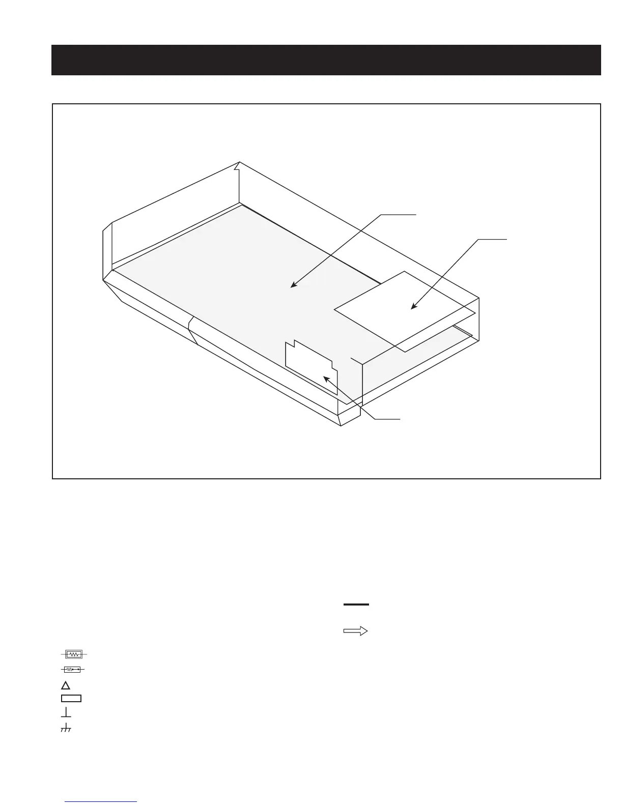
3-1. CIRCUIT BOARDS LOCATION
• All capacitors are in µF unless otherwise noted.
pF: mmF 50 WV or less are not indicated except for electrolytic and
tantalums.
• All electrolytics are 50V unless otherwise specifi ed.
• Indication of resistance, which does not have one for
rating electrical power, is as follows:
Pitch: 5mm
Rating electrical power 1/4W (CHIP: 1/10W)
• All resistors are in ohms.
KW = 1000W • MW = 1000KW
• : nonfl ammable resistor
•
: fusible resistor
•
: internal component
•
: panel designation and adjustment for repair
•
: earth-ground
•
: earth-chassis
• All variable and adjustable resistors have characteristic
curve B, unless otherwise noted.
• All voltages are in Volts
• Readings are taken with a 10M ohm digital multimeter.
• Readings are taken with a color-bar signal input.
• Voltage variations may be noted due to normal production tolerance.
• * : cannot be measured
•
: B + Line
•
-----
: B - Line
•
: Signal path
SECTION 3: DIAGRAMS
A Board
SC2
Board
HB Board
 Loading...