– 35 – – 36 – – 38 –– 37 –
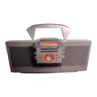
ZS-D55
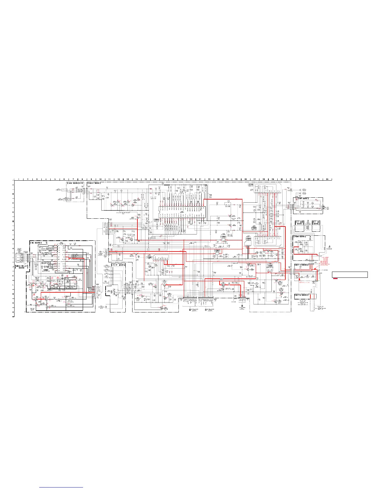
6-5. SCHEMATIC DIAGRAM (MAIN SECTION)
Note:
• All capacitors are in µF unless otherwise noted. pF: µµF
50 WV or less are not indicated except for electrolytics
and tantalums.
• All resistors are in Ω and
1
/
4
W or less unless otherwise
specified.
Note: The components identified by mark 0 or dotted
line with mark 0 are critical for safety.
Replace only with part number specified.
• : B+ Line.
• Power voltage is dc 12V and fed with regulated dc power
supply from external power voltage jack.
• Voltages and waveforms are dc with respect to ground
under no-signal (detuned) conditions.
no m ark : FM (COMMON), TAPE PLAY (TAPE SECTION)
( ) : REC
• Voltages are taken with a VOM (Input impedance 10 MΩ).
Voltage variations may be noted due to normal produc-
tion tolerances.
• Waveforms are taken with a oscilloscope.
Voltage variations may be noted due to normal produc-
tion tolerances.
• Circled numbers refer to waveforms.
• Signal path.
F : FM
E : PB
a : REC
J : CD
z
Refer to page 39 for Waveforms.