2
3 4 5 6
A
1
B
C
IC1
IC2
13
(13)
1-676-535-
A
CONTROL
BOARD
CNP804
(Page 45)
B
AUDIO
BOARD
CNP309
(Page 33)
02
TP
(VT)
L3
MW/LW
FERRITE-ROD
ANTENNA
D3
T1
T2
ANT1
FM
TELESCOPIC
ANTENNA
TUNER BOARD
R64
R16
R43
C45
C25
C46
C7
C5
R42
R7
R18
R12
R9
R19
R17
JC13
JC25
JC6
JC7
JC4
JC3
R22
C1
C6
C67
C40
C3
C2
Q44
BCE
Q43
ECB
Q41
ECB
Q42
ECB
Q12
ECB
Q14
BCE
CT5
DGS
Q61
L3-1L3-2
JC45
– 53 – – 54 –– 51 – – 52 –
ZS-D55
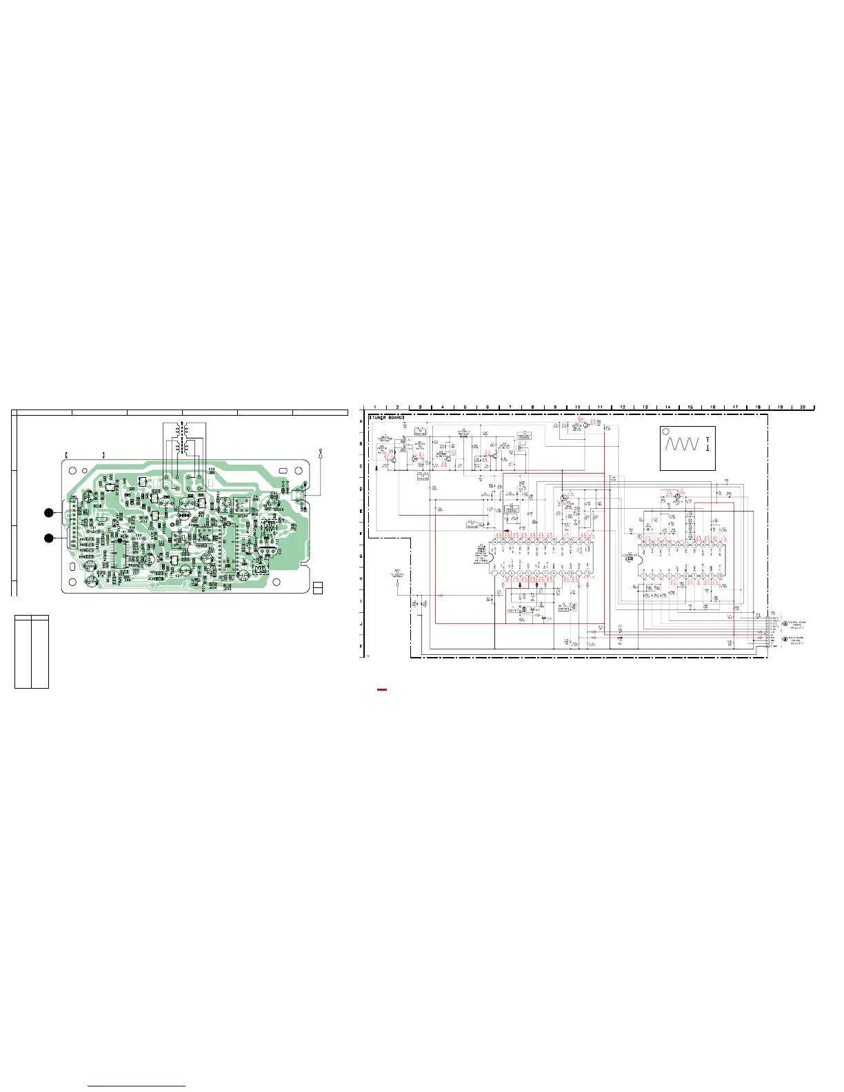
6-10. PRINTED WIRING BOARDS (TUNER SECTION)
6-11. SCHEMATIC DIAGRAM (TUNER SECTION)
Note:
• All capacitors are in µF unless otherwise noted. pF: µµF
50 WV or less are not indicated except for electrolytics
and tantalums.
• All resistors are in Ω and
1
/
4
W or less unless otherwise
specified.
•
f
: internal component.
• : B+ Line.
• H : adjustment for repair.
Note:
• X : parts extracted from the component side.
• b : Pattern from the side which enables seeing.
(The other layers' patterns are not indicated.)
r
Waveform (TUNER Section)
1
IC2 w; (X OUT)
VOLT/DIV : 0.5 V AC
TIME/DIV : 5 µsec
1.5Vp-p
75 kHz
• Power voltage is dc 12V and fed with regulated dc power
supply from external power voltage jack.
• Voltages and waveforms are dc with respect to ground
under no-signal (detuned) conditions.
no mark : FM
():MW
<>:LW
D1 B-4
D2 B-4
D3 B-4
D10 B-5
D11 B-5
IC1 C-4
IC2 C-2
Q12 C-3
Q14 B-2
Q41 B-3
Q42 B-4
Q43 B-3
Q44 B-3
Q61 B-2
Ref. No. Location
r
Semiconductor
Location
• Voltages are taken with a VOM (Input impedance 10 MΩ).
Voltage variations may be noted due to normal produc-
tion tolerances.
• Waveforms are taken with a oscilloscope.
Voltage variations may be noted due to normal produc-
tion tolerances.
• Circled numbers refer to waveforms.
• Signal path.
F : FM
f : AM
 Loading...