UM2407 Rev 2 43/50
UM2407 Extension connectors
49
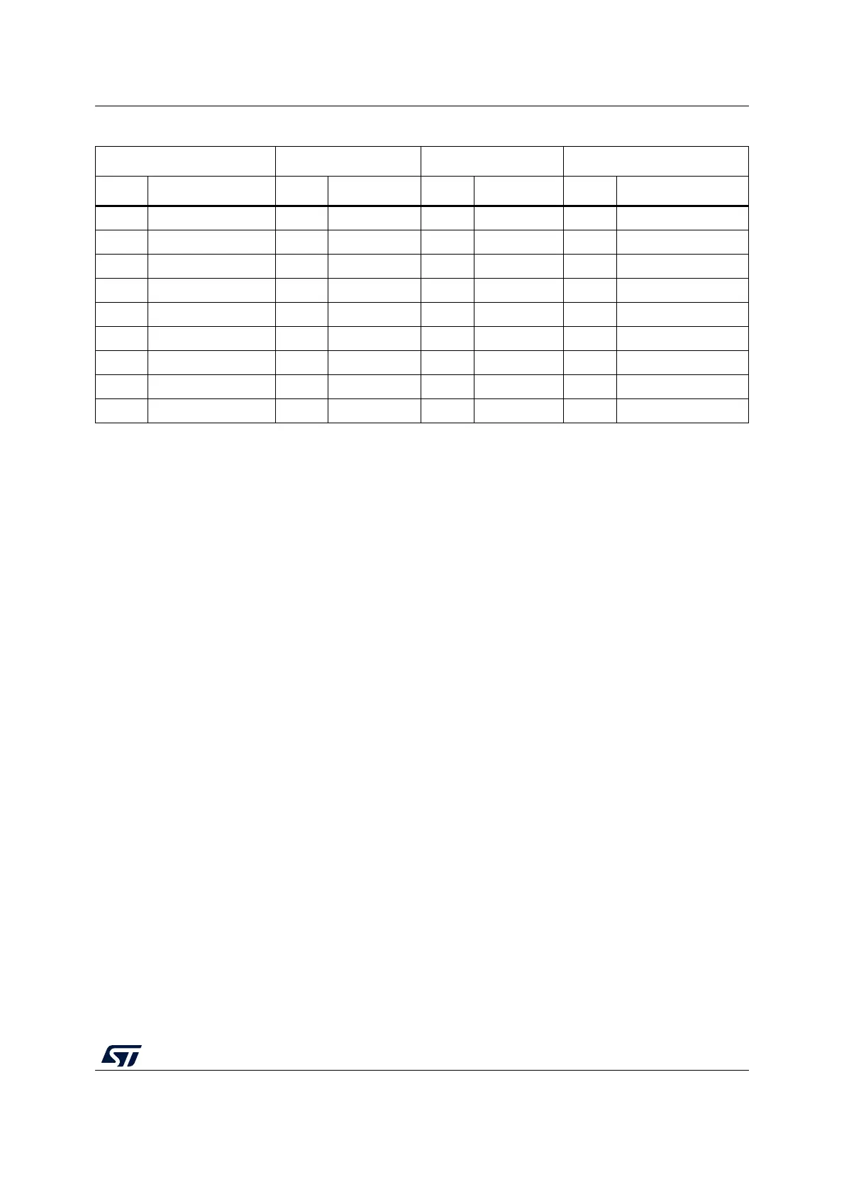
53 PF0 54 PF8 53 PE15 54 GND
55 PD1 56 PF9 55 PE13 56 PE11
57 PD0 58 PG1 57 PF13 58 PF3
59 PG0 60 GND 59 PF12 60 PF15
61 PE1 62 PE6 61 PG14 62 PF11
63 PG9 64 PG15 63 GND 64 PE0
65 PG12 66 PG10 65 PD10 66 PG8
67 NC 68 PG13 67 PG7 68 PG5
69 PD9 70 PG11 69 PG4 70 PG6
1. The default state of BOOT0 is 0. It can be set to 1 when a jumper is plugged on the pins 5-7 of CN11.
2. 5V_USB_STLK is the 5 V power coming from the ST-LINKV3 USB connector that rises before and it rises before the +5 V
rising on the board.
3. PA13 and PA14 are shared with SWD signals connected to STLINK-V3. It is not recommended to use them as I/O pins.
Table 22. ST morpho connector pin assignment (continued)
CN11 odd pins CN11 even pins CN12 odd pins CN12 even pins
Pin nbr Pin name Pin nbr Pin name Pin nbr Pin name Pin nbr Pin name

 Loading...