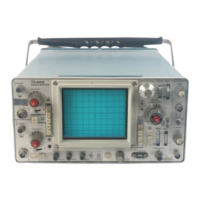
Circuit Description-465
Power Input
Power
is
applied
to
the
primary
of
transformer
T1501
through
Line Fuse
F1501,
POWER switch
S1501,
Thermal
Cutout
S1502,
Line Voltage
Selector
switch
S1503,
and
the
Regulating Range Selector Assembly. Line Voltage Selector
switch
S1503
connects
the
split
primaries
of
T1501 in
parallel for 115-volt nominal
operation,
or
in
series for
230-volt nominal
operation.
Line Fuse F1501 should be
changed
to
the
correct
value
to
provide
the
correct
protection
for each nominal line voltage
(current
rating
of
fuse for 230-volt
operation
is
one-half
the
current
rating of
fuse for 115-volts).
The vacant windings
between
pins
10, 11,
and
12
of
T1501 are intended for use with
the
optional Inverter
Circuit Board (Option 7). This allows
the
instrument
to
be
operated
from an external
DC
power
source
or
an
1106
Power
Supply.
Secondary Circuit
The
-8
volt, +5 volt,
+15
volt, and +55 volt supplies are
series-regulated supplies. U
1524A
and
B
and
U
1554A
and B
are high-gain amplifier cells
with
differential inputs. These
amplifiers
monitor
voltage variations
in
the
output
voltages.
For
SN
B080000
and
up,
a regulated
+110
V supply
is
provided
in
addition
to
the
unregulated
+120
V supply.
Both are derived from
the
terminal 14,
15,
and 16 winding
of
T1501 and
the
full wave bridge rectifier CR 1511.
The
+11 O V regulated
supply
is
referenced
to
the
+55 V
re-
gulated
supply
via
56
V zener
diode
VR1515
and
CR1514
to
the
base
of
series regulator
transistor
01516.
01516
collector
is
fed from
the
+120
V
supply
through
CR1516.
R1516
shunts
01516
to
provide additional
+110
V supply
current.
01518
provides
short
circuit
protection
by limiting
the
current
through
01516
during
overload
conditions.
3-20
Below
SN
B080000,
the
+120
V unregulated supply
functions
in
place
of
the
+110V
and
+120V
supplies of
~
later
production.
This
+120
V
supply
includes SCR
01514
~·
to
provide over-voltage
protection
for
the
various
+120
V
loads
in
the
event
of
higher
than
specified line voltage levels.
This
01514
"Crowbar"
circuit
places a
short
across the
T1501 secondary winding which will cause fuse F1501 to
blow within
40
milliseconds if
the
line voltage exceeds
the
range selected on
the
T1501 primary
taps.
Fuse F 1501
should always be replaced
with
the
specified value
to
pro-
tect
01514.
If
01514
is
destroyed
due
to
too
hig/1
F1501
value,
the
+120
V supply
can
rise
to
about
160
V and
possibly damage
components
in
the
+120
V load circuitry.
C1510,
C1511,
and R1511
compose
a wave-shaping
circuit
that
provides a sample
of
the
AC voltage present
in
the
secondary of T1501
to
the
trigger
circuitry
for use
in
the
LINE positions
of
the
Trigger SOURCE switches.
CR
1512
provides a relatively fast discharge
path
for C1542
when
instrument
power
is
turned
off.
FAN
MOTOR
CIRCUIT
General
The fan
motor
used
in
the
465
is
a brushless
DC
fan
motor
using
Hall
Effect devices. The fan
motor
circuitry
varies
the
rotational
speed
of
the
fan with variations
in
operating
temperature.
When
the
ambient
temperature
increases,
the
value
of
thermistor
RT1696
reduces. This
biases
01698
on
harder
to
cond,
ct
more
current
through
the
Hall devices. Higher
currents
through
the
Hal
I devices
causes the potential difference
aci-:Jss
them
(for instance,
between pins 6 and 8
of
the
fan)
to
increase. This potential
difference biases
one
of
a pair of transistors on and
the
other
off.
For
instance,
if
pin 8
is
more
positive
than
pin 6
of
the
fan,
O1690A
will be on
and
016900
will be off. The
higher
the
potential difference
between
pin 8 and pin 6
the
harder
the
on
transistor will be
conducting.
The harder the
transistor
is
conducting,
the
faster
the
fan
rotates.
®
C
.

 Loading...