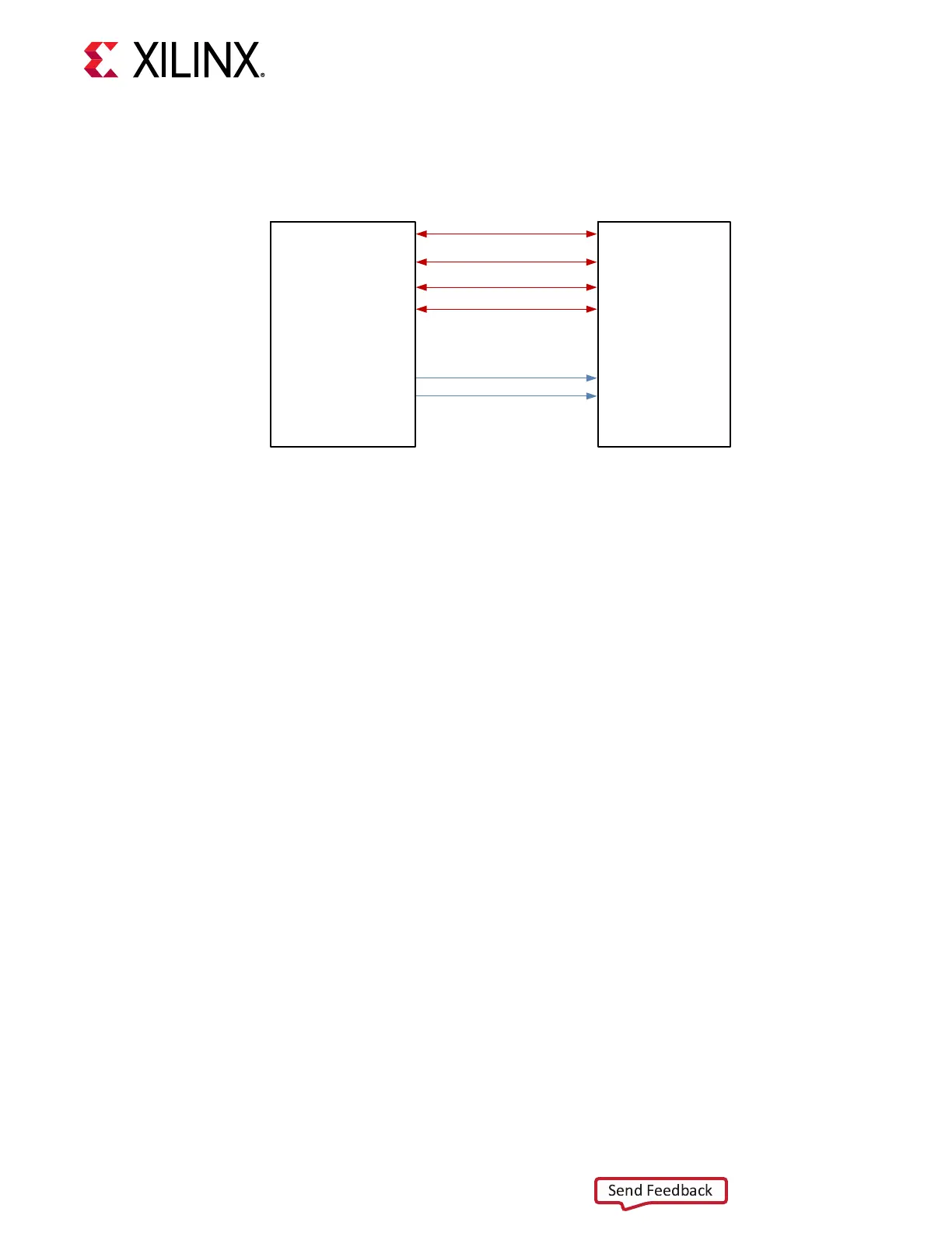
The following gure shows the conguraon ash memory interface.
Figure 5: Configuration Flash Memory Interface
SPI NOR FLASH
MT25QL01G
Spartan-7
FPGA
DQ0
DQ1
DQ2/W#
DQ3/HOLD#/RESET#
C
S#
FLASH_DQ[0]
FLASH_DQ[1]
FLASH_DQ[2]
FLASH_DQ[3]
FLASH_CLK
CS#
U1
X22788-042619
The detailed FPGA connecons for the feature described in this secon are documented in the
SP701 board XDC le, referenced in Appendix B: Xilinx Design Constraints.
SP701 JTAG Chain
[Figure 2, callout 13]
The SP701 JTAG chain has the following components:
• J5 USB micro-AB connector connected to U6 FT4232HQ USB-JTAG bridge
• U1 XCS700 FPGA
• J21 FMC LPC connector
• J3 2x7 2 mm shrouded, keyed JTAG pod at cable connector
The SP701 board JTAG chain is shown in the following gure.
Chapter 3: Board Component Descriptions
UG1319 (v1.0) July 12, 2019 www.xilinx.com
SP701 Board User Guide 19

 Loading...


