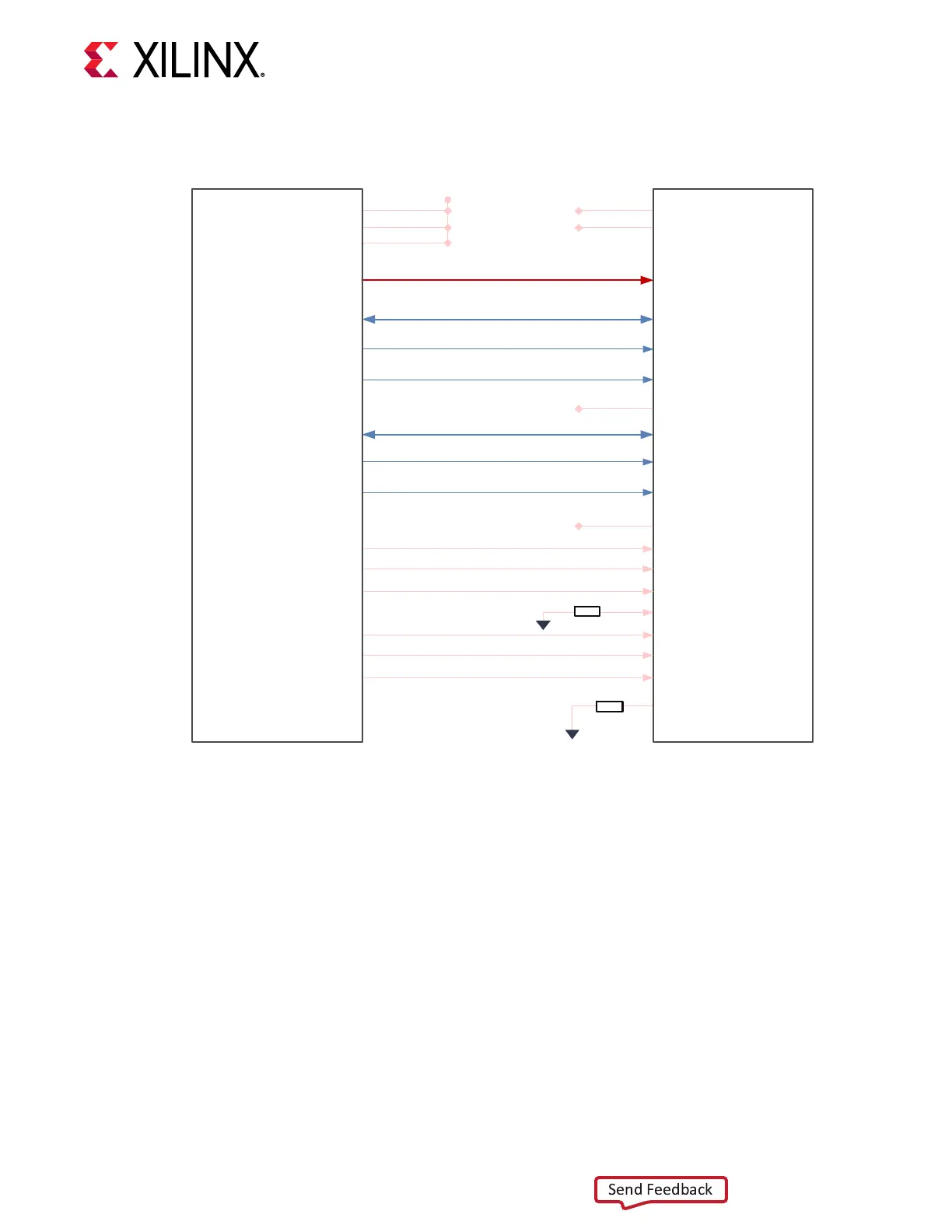
Figure 4: DDR3L Memory Interface
DDR3L SDRAM
MT41K256M16TW-
107cc
Spartan-7
FPGA
A[14:0]
DQ[7:0]
DQ[15:8]
UDM
UDQS/UDQS#
LDM
LDQS/LDQS#
CK/CK#
CKE
BA[2:0]
CS#
ODT
RAS#, CAS#, WE#
RESET#
240E
ZQ
VDD
VDDQ
VREFCA
VREFDQ
1.35V
1.35V
0.675V
0.675V
VDDO_34
VDDO_34
VDDO_34
1.35V
100E
U12U1
X22787-042619
For more details, see the Micron MT41K256M16TW-107 data sheet at the Micron Technology
website.
The detailed FPGA connecons for the feature described in this secon are documented in the
SP701 board XDC le, referenced in Appendix B: Xilinx Design Constraints. For more
informaon, see the Zynq-7000 SoC and 7 Series Devices Memory Interface Soluons (UG586).
Quad SPI Flash Memory
[Figure 2, callout 2]
A single Micron MT25QL01GBBBESF-0SIT 1 Gb serial NOR Flash memory (U3) holds the boot
images for the XC7S100 device. The Spartan-7 conguraon clock is 66 MHz resulng in a
typical conguraon me of 112 ms. This memory can also be used for user data.
Chapter 3: Board Component Descriptions
UG1319 (v1.0) July 12, 2019 www.xilinx.com
SP701 Board User Guide 18

 Loading...


