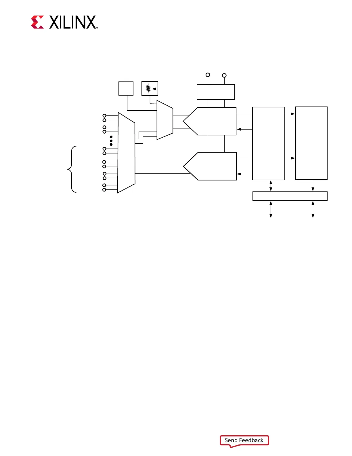
Figure 23: XADC (SYSMON) Block Diagram
Mux
VP_0
VREP_0
Die
Temperature
VCCINT
VCCAUX
VCCBRAM
VCCPINT
VCCPAUX
VCCO_DDR
VREFN_0
Mux
Temperature
Sensor
Supply
Sensors
VN_0
VAUXP[0]
VAUXN[0]
12-bit,
1 MSPS
ADC A
°C
VAUXP[12]
VAUXN[12]
VAUXP[13]
VAUXN[13]
VAUXP[14]
VAUXN[14]
VAUXP[15]
VAUXN[15]
12-bit,
1 MSPS
ADC B
64 x 16 bits
Read/Write
64 x 16 bits
Read Only
Control
Registers
Status
Registers
On-Chip Ref
1.25V
JTAG
FPGA
Interconnect
External
Analog
Inputs
DRP
X17015-070719
It is not necessary to instanate the XADC in a design to access the on-chip monitoring
capability. However, if the XADC is not instanated in a design, the only way to access this
informaon is through the JTAG test access port (TAP). To allow access to the status registers
(measurement results) from the FPGA logic, the XADC must be instanated.
The following gure shows the SYSMON implementaon and SYSMON header J24, a 2x10
shrouded male pin header. Jumper J26 is provided to select internal reference or external
reference.
Chapter 3: Board Component Descriptions
UG1319 (v1.0) July 12, 2019 www.xilinx.com
SP701 Board User Guide 42

 Loading...


