3 - 9
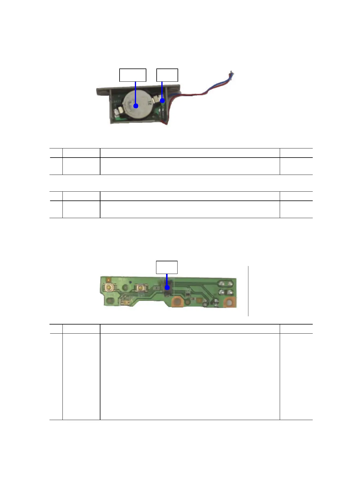
2.4 Coin Battery Unit
J1 (Logic board I/F)
No.
Signal name
Function Input/Output
1Vdd Real Time Clock (RTC) IC drive power supply OUT
2GND GND
BAT1 (Coin battery I/F: Battery holder)
No.
Signal name
Function Input/Output
1
−
Coin battery negative terminal
2
+
Coin battery positive terminal IN
2.5 Panel Board Ass’y
J1 (Logic board I/F)
No.
Signal name
Function Input/Output
1LED_A LED drive power supply IN
2LED_RSM Error LED IN
3LED_PWR Power LED IN
4POWER Power key OUT
5RESUME Resume key OUT
6GND GND
7PES PE sensor OUT
8VSEN_5V PE sensor drive power supply IN
9ASFS ASF sensor OUT
10GND GND
J1
BAT1
J1
 Loading...