— 15 —
VREG,V1~V4
Output
for LCD
driver
PDB
Power supply chip
SC371015FU
VDD2
VDD1
VO1
GND
(Pin2)
(Pin1)
(Pin19)
(Pin31)
VIN
GND
VDD
VDDVOT
KAC
KIO
ADDRESS BUS
2 MHz
VDD1
ON
MAIN SWITCH
SW
GND
VDD
(Pin53)
(Pin54)
(Pin41)
2
VDD
(Pin69)
"H"
"H"
ADDRESS
DATA
"H"
VDD
1
"L"
OSCOOSCI
INIT1
(Pin70)
INT0
V2ON
Gate array
ON
VDD
DATA BUS
(Pin40)(Pin45)
(Pin36)
"L"
(Pin31)
(Pin34)(Pin32)
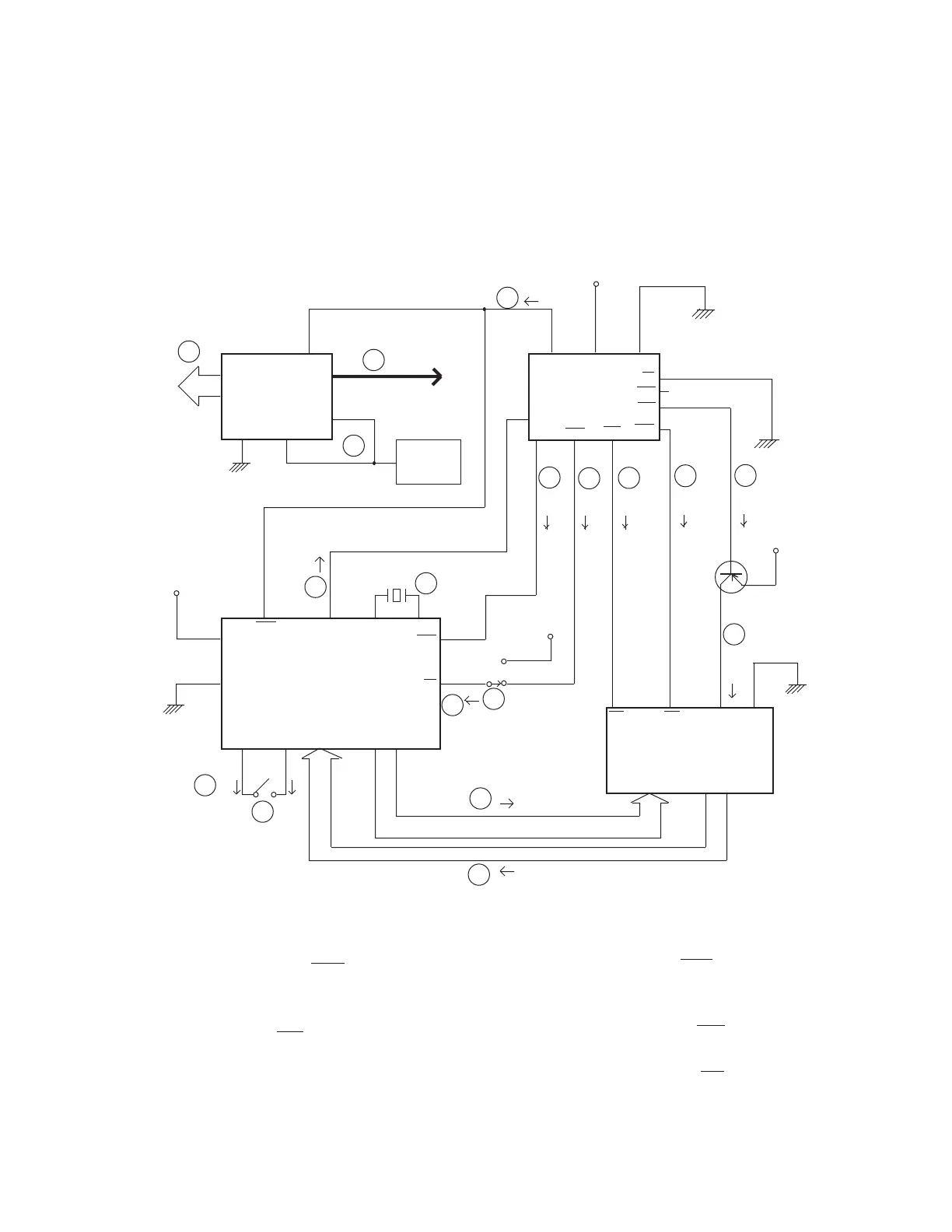
10-1. System chart
Generally, SF-8500 is working with the following steps.
2. Output VDD (4.5V).
1. Supply 5V to VDD1 and VDD2.
OFF
10. CIRCUIT EXPLANATIONS
CPU
HD62076C02
Power supply
Circuit
LSO
"H"
SWO
"L"
(Pin32)
(Pin22)
3
4
6
5
7
8
9
10
11
12
µPD23C4001EBGW-304
(Operation program)
ROM
LSI
(Pin26)
MON
µPD65005GC-566-3B6
VOB
(Pin25)
VDD
GNDVCC
14
(Pin3)
(Pin1)
"H"
"L"
13
(Pin2)
OEO
(Pin40)
(Pin27)
"L"
15
(Pin43)
(Pin39)
RSO
(Pin49)
"L"
16
17
18
CEOE
(Pin24)
(Pin22)
3. Output "L" from SWO terminal.
5. Main switch ON.
6. Input "L" to SW terminal.
7. Output "L" from KAC terminal.
8. Push power on button switch.
4. Output "H" from LSO terminal.
9. CPU oscillation is generated.
10. Output "H" from V2ON terminal.
13. Output "L" from VOB terminal.
15. Gate array sends ROM output
enable signal from OE terminal.
18. CPU receives data from ROM.
11. Output "H" from VOT terminal.
12. Output all LCD drive voltages.
14. Apply VDD to ROM.
16. Gate array sends ROM Chip enable
enable signal from CE terminal.
17. CPU sends address to ROM.
Transistor Q1
(Pin7)
(Pin33)
 Loading...