— 24 —
10-7. Operation program ROM pin discriptions (µPD23C4001EBGW-304)
10-8. RAM pin discriptions (M5M51008AFP-10LL)
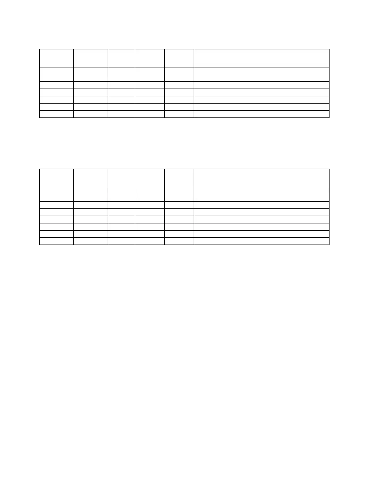
Pin No. Name In/Out Status Status Description
of OFF of ON
2~12,23, A0~A18 In L Pulse Address bus line (A0~A14, RA15~RA18)
25~31
13~15, 17~21 O0~O7 Out L Pulse Data bus line (IO0~IO7)
16 GND In L L GND terminal
22 CEB In H Pulse Chip enable signal from Gate array
24 OEB In L Pulse Output enable signal from Gate array
1, 32 N.C., VCC In L H VDD terminal
Pin No. Name In/Out Status Status Description
of OFF of ON
2~12,23, A0~A16 In L Pulse Address bus line (A0~A14, RA15, RA16)
25~28, 31
13~15, 17~21 O0~O7 Out L Pulse Data bus line (IO0~IO7)
16 GND In L L GND terminal
22 CS1 In H Pulse Chip enable signal from Gate array
24 OEB In L Pulse Output enable signal from Gate array
1, 32 N.C., VCC In L H VDD terminal
29 WEB In H Pulse Write enable signal from CPU
 Loading...