— 23 —
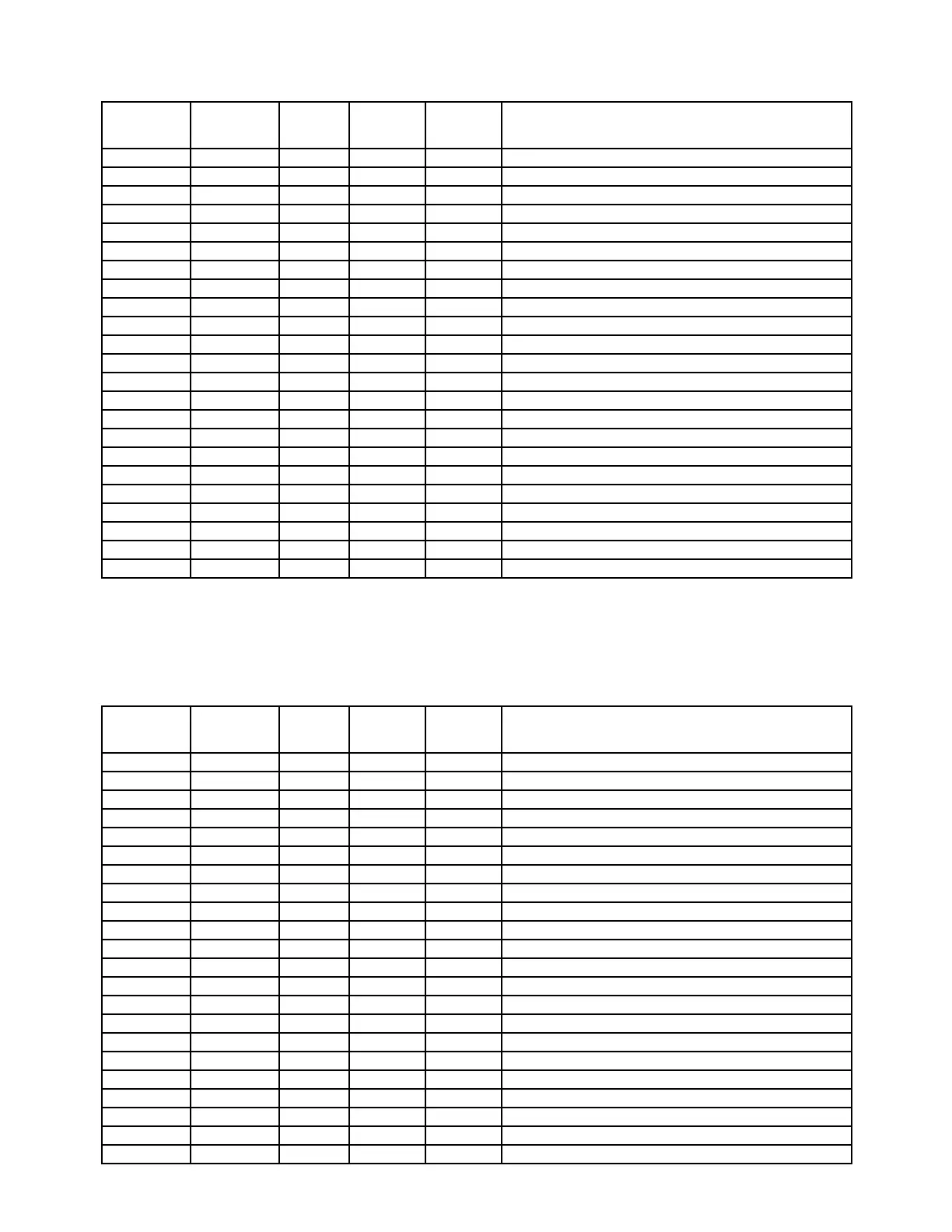
10-6. Character generator ROM pin descriptions (HD62063B01)
Pin No. Name In/Out Status Status Description
of OFF of ON
1, 7~12, 23 NC ** ** ** Not used
2 BLD In L L Not used (Battery voltage detection terminal)
3 VOSC In 3V 3V Connected capacitor
4, 20 GND In L L GND terminal
5, 6 OSI/OSO In Pulse Pulse Exterminal clock terminal (32.768 KHz)
13 TNL Out ** ** Not used
14, 19 IN1+, IN2+ In H H Connected to VDD
15, 32 VSS1, VSS2 In L L GND terminal
16, 21 IN1-, IN2- In H H Connected to VDD
17, 22 OUT1, OUT2 Out ** ** Not used
18 TNH Out ** ** Not used
24 IN In L Pulse Power on key input terminal
25 OUT Out H Pulse K10 terminal for power on
26` 27 BZ1, 2 Out L L Buzzer signal
28 INT Out H H Interrupt signal for alarm clock (alarm time…"L")
29, 30 CEH, CEL Out H Pulse RAM chip select signal
31 CED In H Pulse Chip enable signal from CPU
33 EN In L H Enable signal (Buzzer off…"L")
34~37 IO3~IO0 In/Out L Pulse Data bus line (IO0~IO3)
38~42 A0~A3, A15 In L Pulse Address bus line (A0~A3, A15)
43 WEB In H Pulse Write signal
44 CSB In H Pulse Chip select signal
Pin No. Name In/Out Status Status Description
of OFF of ON
3 SUB IN In +3V +3V Back-up battery detection input
4 SUB OUT Out H H Back-up battery detection output (less than 2.5V…"L")
5 V COMP0 Out H H Battery detection signal (less than 3.7V…"L")
6 V COMP1 Out H H Battery detection signal (less than 4.4V…"L")
7 V COMP2 Out H H Battery detection signal (less than 4.7V…"L")
8 VSS Out H -7V LCD drive power VREG
9 V1 Out L 3V LCD drive power V1
10 V2 Out L 2V LCD drive power V2
11 V3 Out H -5V LCD drive power V3
12 V4 Out H -6V LCD drive power V4
13~16 VDIV1~4 ** H Wave Voltage drividing terminal for LCD drive power
17 C1N ** GND Wave Negative terminal for doubler capacitor C3
18 C2P ** 3V Wave Not used
20 C1P ** 3V Wave Positive terminal for doubler capacitor C3
21 C2N ** GND Wave GND
23 SUB CONT In L L Back-up battery detection clock input
24 EROUT Out H Wave LCD drive basic voltage output
25 VFB ** H Wave LCD drive basic voltage input
26 MIN In 5V 5V LCD drive MIN voltage setting terminal
27 MAX In %v 5V LCD drive MAX voltage setting terminal
28 UPDOWN In H H LCD contrast control signal input (Up/Down)
29 CLOCK In L L LCD contrast clock signal input
30 SET In H H Switch signal for contrast ("L"…software, "H"…hardware)
 Loading...