3.3V 2,12,19,20,22,23,24,26,32,33,38,39,40
U2 5 A
74LVC08PW
1
2
3
147
POWER GOOD & RESET
SB_PC IRST#12,21
C7 2 6
*.01U_16 V_ X7R _0 4
S3AUXSW#
LID_SW# 20,27
Z2912
R2 94
*10K_04
3. 3 V
M_ BTN #40
R1 10K_04
0
R2 8 2
*10K_04
R3 3 8 33 _0 4
U2 5 C
74LVC08PW
9
10
8
147
J_ S W 1
85201-04051_R
1
2
3
4
R273 *10m il_short
1. 5 V _ P W R G D39
1
Z2901
M_ BT N#
R3 3 5 33 _0 4
J_SW1
1
3.3V
U2 5 D
74LVC08PW
12
13
11
147
KBC_SUSB # 27
C 740 .01U_16V_X7R _04
U1 9
* 7 4 A H C 1G 08 G W
1
2
5
4
3
SATA HDD
C430
* .1U_16V_04
5VS
Q1 3
*2N7002W
G
DS
S4/S5
POWER SWITCH CONNECTER
1. 8 V _ P W R G D40
D EL AY_ PW RG D6,37
1
C 742 .01U_16V_X7R _04
SIS????
?????
Con ne cto r
PSON#22
SA TAR XP0 2 3
PCI_ RST # 28 ,3 2 ,33
NB_ RST # 6,1 1
Z2908
PSU1, PSU2
C4 1 5
*.1U_16V_04
0
3. 3V
PIN GN D1 ~ 2 =G ND
5VS 19,20,29,30, 32,34,35
C699
1 U _1 0 V _0 6
SB_PW R OK 2 0,22
LID SWITCH IC
C4 2 0
.1U_10V_ X7R _0 4
LP C_ RST # 2 7,3 3
S0/S1
SATARXN0_ R
3
D0 3A
1
3.3V S 6,10,11,19,20,21,22,23,24,25,27,28,29,30,32,33,34,35,37
Z2903
SA TAT XP0 2 3
+
C7 09
10 0U_6.3V_ B2
C 507 * .1U _10V_X7R_04
C7 2 7
*10U_10V_08
Q1 5
*2N7002W
G
DS
R342
100K_04
POWER MANAGMENT
2
3. 3 V
SATATXN 0_ R
R3 67
10 K _ 0 4
R2 7 6
*4 .7 K _0 4
R2 7 2
*4 .7 K _0 4
1
D03 A
Q1 4
*2N7002W
G
DS
C4 2 1
.1U_10V_ X7R _0 4
4
Z2904
R3 3 0 33 _0 4
3.3V
S3
Z291 0
R2 7 7
100K_04
R275 *10m il_short
3.3V
NB_ S3 A UXS W #5
SA TAT XN0 23
R279 *10m il_short
Z2905
Z2902
Z290 7
C7 1 1
10U _10V_08
1.05 VS_PW R GD39
SUSB# 12, 25,28,33,35,39,40
LID_SW#
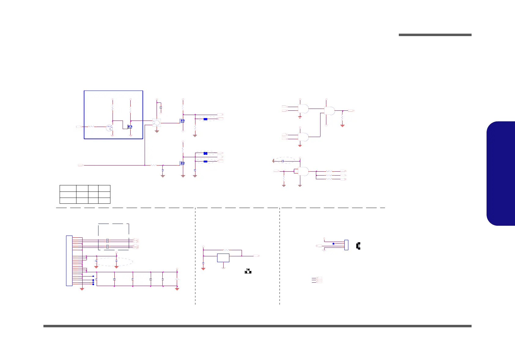
VCORE Power Good delay
3ms and Notice SB
D03 A
3.3V
3. 3 V
C4 0 9
*.1U _16V_04
R2 8 0
*100K_04
J_ HD D1
91907-0220C
S1
S2
S3
S4
S5
S6
S7
P1
P2
P3
P4
P5
P6
P7
P8
P9
P10
P11
P12
P13
P14
P15
C710
.1U _10V_X7R_04
D03 A
SATATXP0 _ R
Q26
*D TC 11 4 E U A
CE
B
3.3VS
SATARXN0 23
If ne ed PSO N#
th an use d 1 00 K
an d 0 .1U
KBC_SUSC # 27
Z2911
Z2913
PSON#
For NB control and Level shift
All Power Good and
Notice SB
SB_SUSC# 2 2
SB_SUSB# 22
SIGNAL
Close to SIS968
D0 3A
C 735 .01U_16V_X7R _04
1
R4 8 9
*0_04
Z2906
C1
.1U _10V_X7R_04
C 737 .01U_16V_X7R _04
3.3V 3. 3V
SATARXP0_R
U1
MH-2 4 8
1 2
3
VCC O UT
GN D
3. 3 V S
Z290 9
U2 5 B
74LVC08PW
4
5
6
147
 Loading...