EasyManua.ls Logo

Clevo W670SZQ User Manual

Clevo W670SZQ
106 pages
To Next Page IconTo Next Page
To Previous Page IconTo Previous Page
Page #65 background imageLoading...
Page #65 background image
Schematic Diagrams
Processor 7/7- RSVD B - 9
B.Schematic Diagrams
Processor 7/7- RSVD
FC_G6
Has well rPGA EDS
9 OF 9
U26I
RSVD
P10
RSVD
U10
NC
B1
VSS
AR26
VSS
AP27
RSVD_TP
E20
RSVD_TP
E21
RSVD
A2
RSVD
E18
RSVD_TP
AR1
RSVD
K6
RSVD
AM2
RSVD
F5
RSVD
AM26
RSVD
AM27
CFG_19
AP23
CFG_17
AP21
CFG_18
AR23
CFG_16
AR21
CFG_RCOMP
AT31
RSVD_TP
D23
RSVD_TP
D24
RSVD_TP
B23
RSVD_TP
C23
CFG_15
AP25
CFG_14
AN 26
CFG_13
AN 25
CFG_9
AT23
CFG_8
AR 24
CFG_7
AN 23
CFG_6
AT25
RSVD_TP
B35
RSVD_TP
C35
VCC
F25
RSVD
AL29
RSVD
AL30
RSVD
W33
RSVD_TP
A35
RSVD_TP
A34
RSVD
AD 10
RSVD_TP
AT2
RSVD_TP
AT1
CFG_12
AP26
CFG_11
AP24
CFG_10
AN 20
RSVD_TP
W29
RSVD_TP
W28
TESTLO
G26
RSVD
AR33
FC
G6
RSVD_TP
AL25
RSVD_TP
W30
RSVD_TP
W31
TESTLO
W34
CFG_0
AT20
CFG_1
AR 20
CFG_4
AT22
CFG_5
AN 22
CFG_3
AP22
CFG_2
AP20
VSS
AL31
VSS
AL32
H_CPU_RSVD40
R67 *1K_04
R66 * 1K_04
R64 * 1K_04
R378 *1K_04
R63 *1K_04
R28
*1K_04
Haswell Processor 7/7 ( RESERVED )
CFG3
CFG5
CFG4
CFG2
CFG6
CFG7
R359 49.9_1%_04
R357 49.9_1%_04
R384 49.9_1%_04
(Default)
NOTE:
PHYSICAL_DEBUG_ENABLED (DFX PRIVACY)
0 : ENABLED SET DFX ENABLED BIT IN DEBUG INTERFACE MSR
1 : DISABLED
(Default)
CFG3
DEFENSIVE PULL DOWN SITE
CFG5
CFG4
CFG2
CFG2
CFG6
CFG[6:5]
PCI EXPRESS STATIC LANE REVERSAL FOR ALL PEG PORTS
1: (DEFAULT)NORMAL OPERATION;
LANE# DEFINITION MATCHES
0: LANE REVERSAL
PCIE Port Bifurcation Straps
11: DEVICE1 FUNTION 1, DEVICE 1 FUNCTION2 DISABLED
10: DEVICE1 FUNCTION1 ENABLED DEVICE1 FUNCTION 2 DISABLED
01: DEVICE 1 FUNCTION 1 DISABLED, DEVICE 1 FUNCTION 2 ENABLED
00: DEVICE 1 FUNCTION 1 ENABLED, DEVICE 1 FUNCTION 2 ENABLED
CFG7
CFG4
CFG Straps for Processor
DISPLAY PORT PRESENCE STRAP
1: DISABLED;
NO PHYSICAL DISPLAY PORT ATTACHED
TO EMBEDDED DISPLAY PORT
0:ENABLED; AN EXTERNAL DISPLAY PORT DEVICE
AN EXTERNAL DISPLAY PORT DEVICE IS CONNECTED
TO THE EMBEDDED DISPLAY PORT
VC CIN5,41
VCCIN
PM_PCH_PWROK 22,36
CFG_RCOMP
R68 1K_04
FC_G6
H_CPU_RSVD30
R29
*2K_1%_04
NOTE:
RESERVE THIS CIRCUIT FOR FUTURE COMPATIBILITY
Sheet 8 of 46
Processor 7/7-
RSVD

Table of Contents

Question and Answer IconNeed help?

Do you have a question about the Clevo W670SZQ and is the answer not in the manual?

Clevo W670SZQ Specifications

General IconGeneral
BrandClevo
ModelW670SZQ
CategoryLaptop
LanguageEnglish

Summary

Preface to Notebook Computer Service Manual

Notice and Trademarks

Publication notice, disclaimer of liability, and list of registered trademarks.

About this Manual

Explains the manual's purpose, intended audience, and scope for service.

Important Safety Instructions

Essential safety precautions to reduce risks of fire, electric shock, and injury.

Caution: Laser Class 1 Product

Specific warning regarding the computer's optical device being a Laser Class 1 product.

FCC Compliance Statement

Device compliance with FCC Rules regarding interference.

Care and Operation Guidelines

Guidelines for proper handling and care to prevent damage to the notebook.

Power Safety Precautions

Requirements and safety guidelines for using the computer's power adapter.

Battery Precautions and Guidelines

Critical precautions for battery handling, storage, and guidelines.

Battery Disposal Information

Information on proper battery recycling and disposal procedures.

Related Documents and System Startup

References to other manuals and steps for initial system startup.

Chapter 1: Introduction to Notebook Components

Introduction Overview

Overview of the manual's scope for servicing and upgrading the notebook computer.

Technical Specifications

Detailed technical specifications for processor, memory, storage, display, and more.

External Component Locations

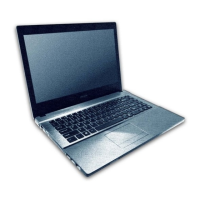
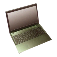
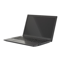
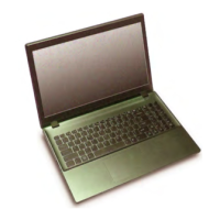
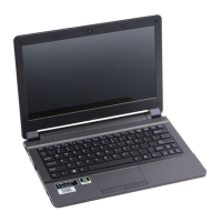
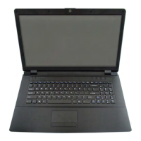
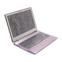
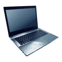
Identification of external parts on the top, sides, rear, and bottom views.

Mainboard Overview

Identification of key parts and connectors on the mainboard's top and bottom.

Chapter 2: Disassembly Procedures

Disassembly Overview and Tools

Introduction to disassembly, including necessary maintenance tools.

Connections and Maintenance Precautions

Description of internal connections and crucial maintenance precautions.

Disassembly Steps Summary

A reference table listing disassembly steps and their page numbers.

Removing the Battery

Step-by-step instructions for removing the notebook battery.

Removing the Keyboard

Step-by-step instructions for removing the notebook keyboard assembly.

Removing the Hard Disk Drive

Instructions for removing the hard disk drive for upgrade or replacement.

Removing the Optical Drive

Step-by-step instructions for removing the CD/DVD optical drive.

Removing System Memory (RAM)

Instructions for removing or replacing system memory modules.

Processor Removal and Installation

Detailed guide for removing and installing the CPU.

Removing the Fan Unit

Instructions for removing and replacing the computer's internal fan.

Removing Wireless LAN Module

Step-by-step instructions for removing the wireless LAN module.

Removing MSATA Module

Instructions for removing the MSATA storage module.

Removing the CCD

Step-by-step instructions for removing the CCD module.

Appendix A: Part Lists and Illustrations

Part List Illustration Location

Index table indicating where to find illustrations for component part numbers.

Appendix B: Schematic Diagrams Overview

Version Note

Important note regarding schematic diagram versions and service center contact.

System Block Diagram

High-level overview of the notebook's system architecture and connections.

Processor Schematics

Schematics for processor DMI, FDI, PEG, CLK, MISC, and DDR3 interfaces.

Memory Slot Schematics

Schematics detailing the DDR3 SO-DIMM memory slots.

Display Interface Schematics

Schematics for PS8625, Panel, Inverter, and VGA PCI-E interfaces.

Graphics Schematics

Schematics for VGA Frame Buffer interfaces (A and C).

VGA I/O and Related Schematics

Schematics for VGA I/O, NVVDD Decoupling, and CRT/Holes.

Chipset Interface Schematics (Lynx)

Schematics for Lynx Point interfaces (HDA, JTAG, SATA, LPC, SMBUS, SPI, CRT, LVDS, PCI, DISPLAY).

Connectivity Schematics

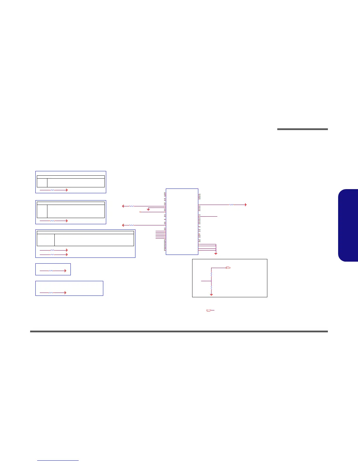
Schematics for 3G, WLAN, PCIE, CON, USB Charge, CCD, TPM, Power Con.

Component and Interface Schematics

Schematics for eSATA/USB3.0, LED, Card Reader, HDD, TP, Audio, USB, HDMI, RJ45.

Audio and Control Schematics

Schematics for the Audio Codec VT1802S and KBC-ITE IT8587.

Power Supply Schematics

Schematics for various power rails including 5VS, 3VS, 1.05V, VDD3/5, 1.5V, VCORE.

GPU and Power Management Schematics

Schematics for NVIDIA GPU power (N14P, NVVDD) and AC adapter/charger.

Board Level Schematics

Schematics for Audio Board, Power Switch Board, and ODD to HDD Board.

Appendix C: BIOS Update Procedures

BIOS Update Prerequisites

Required steps before starting the BIOS update process.

Download and Prepare BIOS Update Files

Instructions for downloading and unzipping BIOS files to bootable media.

Set Boot Order for BIOS Update

Configuring BIOS to boot from an external CD/DVD/USB drive.

Execute BIOS Flash and Restart

Using flash tools to update BIOS and restarting the computer.

Related product manuals