76
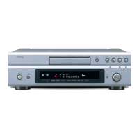
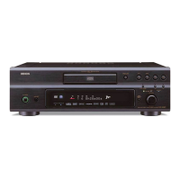
DVD-3910
K4S641632 (MA: IC114)
W986416DH (MA: IC103)
1
2
3
4
5
6
7
8
9
10
11
12
13
14
15
16
17
18
19
20
21
25
24
23
22
V
CC
V
CC
Q
DQ0
V
SS
Q
DQ2
V
SS
Q
DQ6
V
CC
Q
DQ4
BS0
BS1
A10/AP
A0
DQ1
DQ5
V
CC
LDQM
Vcc
WE
CAS
RAS
CS
DQ7
DQ3
26
27
A1
A2
V
SS
VssQ
DQ15
V
CC
Q
DQ13
V
CC
Q
DQ9
V
SS
Q
DQ11
A9
A8
A7
A6
A5
DQ14
DQ10
V
SS
NC
UDQM
CLK
CKE
NC
A11
DQ8
DQ12
A4
Vss
54
53
52
51
50
49
48
47
46
45
44
43
42
41
40
39
38
37
36
35
34
30
31
32
33
29
28
A3
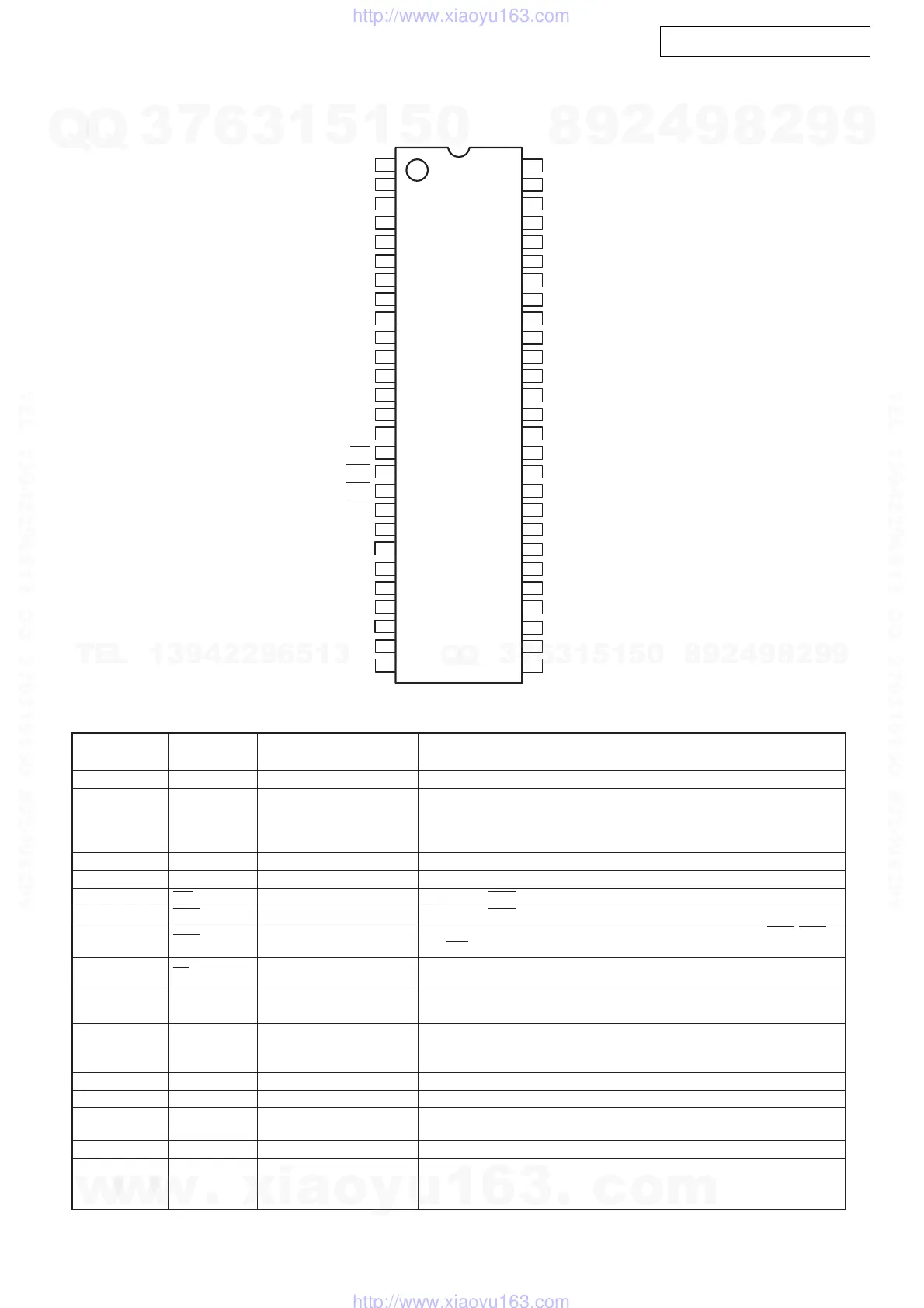
1, 14, 27 VCC Power (+3.3V) Power for input buffers and logic circuit inside DRAM.
2, 4, 5, 7, 8, 10,
11, 13, 42, 44,
DQ0-DQ15 Data Input/Output Multiplexed pins for data output and input.
45, 47, 48, 50,
51, 53
3, 9, 43, 49 VCCQ Power (+3.3V) for I/O buffer Separated power from VCC, to improve DQ noise immunity.
6, 12, 46, 52 VSSQ Ground for I/O buffer Separated ground from VSS, to improve DQ noise immunity.
16 WE Write Enable Referred to RAS.
17 CAS Column Address Strobe Referred to RAS.
18 RAS Row Address Strobe
Command input. When sampled at the rising edge of the clock RAS, CAS
and WE define the operation to be executed.
19 CS Chip Select
Disable or enable the command decoder. When command decoder is
disabled, new command is ignored and previous operation continues.
20, 21 BS0, BS1 Bank Select
Select bank to activate during row address latch time, or bank to read/write
during address latch time.
23~26, 22
Multiplexed pins for row and column address. Row address: A0-A11.
29~35
A0-A11 Address Column address: A0-A7. A10 is sampled during a precharge command to
determine if all banks are to be precharged or bank selected by BS0, BS1.
28, 41, 54 VSS Ground Ground for input buffers and logic circuit inside DRAM.
36, 40 NC No Connection No Connection
37 CKE Clock Enable
CKE controls the clock activation and deactivation. When CKE is low,
Power Down mode, Suspend mode, or Self Refresh mode is entered.
38 CLK Clock Inputs System clock used to sample inputs on the rising edge of clock.
The output buffer is placed at Hi-Z (with latency of 2) when DQM is sampled
39, 15 UDQM, LDQM Input/Output mask high in read cycle. In write cycle, sampling DQM high will block the write
operation with zero latency.
DescriptionFunction
Pin No. Pin Name
Terminal Function
w
w
w
.
x
i
a
o
y
u
1
6
3
.
c
o
m
Q
Q
3
7
6
3
1
5
1
5
0
9
9
2
8
9
4
2
9
8
T
E
L
1
3
9
4
2
2
9
6
5
1
3
9
9
2
8
9
4
2
9
8
0
5
1
5
1
3
6
7
3
Q
Q
TEL 13942296513 QQ 376315150 892498299
TEL 13942296513 QQ 376315150 892498299
http://www.xiaoyu163.com
http://www.xiaoyu163.com
 Loading...