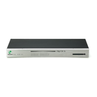
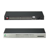
Basic Description
23
"Port Descriptions" on page 25
"Connectors and Blocks" on page 28
"Switches and Push Buttons" on page 35
"Development Board LEDs" on page 37
"Power Jack P15" on page 39
See the following figures for placement of either module onto the development board.
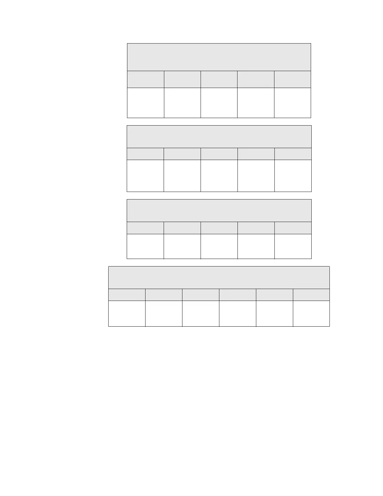
Connectors, Switches and LEDs
Board Description Markers 1-5
1 2 3 4 5
Secondary
Serial Port, P2
Primary Port
LEDs, CR5 -
CR18
GPIO Switch
Bank, SW3
Prototyping
Area, P4
JTAG
Header, P12
Connectors, Switches and LEDs
Board Description (continued) Markers 6-10
6 7 8 9 10
232 Enable
Jumper
Block, P5
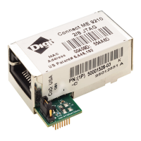
Embedded
Module
Connector,
P10
JTAG
Connector,
P11
Primary
Serial Port, P1
GPIO Port, P7
Connectors, Switches and LEDs
Board Description (continued) Markers 11-15
11 12 13 14 15
Digital I/O
LEDs, CR19 -
CR23
Logic
Analyzer
header, P3
POE Source
LED, CR24
Reset Switch,
SW4
User
Pushbuttons,
SW1 & SW2
Connectors, Switches and LEDs
Board Description (continued) Markers 16-21
16 17 18 19 20 21
Power Jack,
P15
On/Off
switch, SW5
Secondary
Port LEDs
CR1-CR4
-48V DC
output from
module P13
12V output
from PoE
module P14
Current
Measurement
Option P8
 Loading...