EasyManua.ls Logo

Icom IC-7200 Service Manual

Icom IC-7200
135 pages
To Next Page IconTo Next Page
To Previous Page IconTo Previous Page
Page #81 background imageLoading...
Page #81 background image
2 - 4
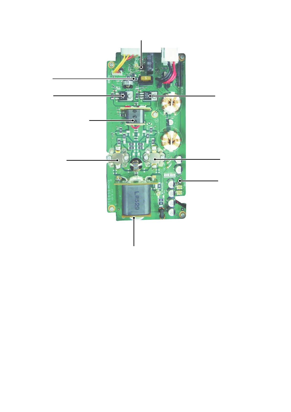
• PA UNIT
COUPLER (For power amp.)
COUPLER (For drive amp.)
PRE DRIVE
(Q1)
DRIVE AMP
(Q3)
PWR AMPLIFIER
(Q5)
FAN CTRL
(Q131)
DRIVE AMP
(Q2)
PWR AMPLIFIER
(Q4)
+8V REG
(IC1)

Other manuals for Icom IC-7200

Questions and Answers:

Icom IC-7200 Specifications

Ports & interfaces IconPorts & interfaces
connector typeUSB B type
interfaceUSB 2.0/1.1
serial speed300/1200/4800/9600/19200 bps
Power IconPower
power supplySelf power
Audio IconAudio
received audio output number of data bit16-bit
received audio output sampling rate8/11.025/16/22.05/32/44.1/48 kHz
modulation input number of data bit16-bit
modulation input sampling rate32/44.1/48 kHz

Summary

CONTENTS

PARTS LIST

Lists all components for the main unit.

BOARD LAYOUTS

Visual diagrams of PC board component layouts.

VOLTAGE DIAGRAM

Schematic showing voltage distribution and connections.

PARTS LIST

BOARD LAYOUTS

LOGIC UNIT (TOP VIEW)

Top-side component layout for the logic unit PC board.

MAIN UNIT (TOP VIEW)

Top-side component layout for the main unit PC board.

RF UNIT (TOP VIEW)

Top-side component layout for the RF unit PC board.

VR-A UNIT (TOP VIEW)

Top-side component layout for the VR-A unit board.

VR-B UNIT (TOP VIEW)

Top-side component layout for the VR-B unit board.

MIC UNIT (TOP VIEW)

Top-side component layout for the MIC unit board.

PHONE UNIT (TOP VIEW)

Top-side component layout for the PHONE unit board.

VOLTAGE DIAGRAM

LOGIC UNIT (LOGIC-1)

Voltage distribution for Logic Unit 1.

LOGIC UNIT (LOGIC-2)

Voltage distribution for Logic Unit 2.

PA UNIT

Voltage distribution for the PA Unit.

MAIN UNIT

Voltage distribution for the Main Unit.

RF UNIT

Voltage distribution for the RF Unit.

FILTER UNIT

Voltage distribution for the Filter Unit.

INTRODUCTION

MODEL VERSION BAND CARRIER POWER

Details model, version, band, and carrier power specifications.

ORDERING PARTS

Guidelines for ordering replacement components.

REPAIR NOTES

SPECIFICATIONS

INSIDE VIEWS

CIRCUIT DESCRIPTION

3-1 RF UNIT

Description of the RF circuit functions.

3-2 MAIN UNIT

Description of the main unit circuits.

3-3 PA UNIT

Description of the PA unit circuits.

3-4 FILTER UNIT

Description of the filter unit circuits.

3-5 VOLTAGE BLOCK DIAGRAM

Block diagram showing voltage distribution.

3-6 PORT ALLOCATIONS

Allocation and description of unit ports.

ADJUSTMENT PROCEDURES

4-1 PREPARATION

Required equipment and common connections for adjustment.

4-2 ADJUSTMENT

Procedures for transmitter and receiver adjustments.

PARTS LIST

MECHANICAL PARTS

BOARD LAYOUTS

LOGIC UNIT

Top-view layout of the logic unit PC board.

VR-A BOARD

Top-view layout of the VR-A board.

VR-B BOARD

Top-view layout of the VR-B board.

MIC BOARD

Top-view layout of the MIC board.

PHONE BOARD

Top-view layout of the PHONE board.

RF UNIT

Top-view layout of the RF unit PC board.

MAIN UNIT

Top-view layout of the MAIN unit PC board.

FILTER UNIT

Top-view layout of the FILTER unit PC board.

PA UNIT

Top-view layout of the PA unit PC board.

GENERAL WIRING

BLOCK DIAGRAM

SCHEMATIC DIAGRAM

LOGIC UNIT

Schematic diagram for the Logic Unit.

VR-A BOARD

Schematic diagram for the VR-A board.

VR-B BOARD

Schematic diagram for the VR-B board.

MIC BOARD

Schematic diagram for the MIC board.

PHONE BOARD

Schematic diagram for the PHONE board.

MAIN UNIT

Schematic diagram for the Main Unit.

RF UNIT

Schematic diagram for the RF Unit.

PA UNIT

Schematic diagram for the PA Unit.

FILTER UNIT

Schematic diagram for the Filter Unit.

Related product manuals