4 - 4
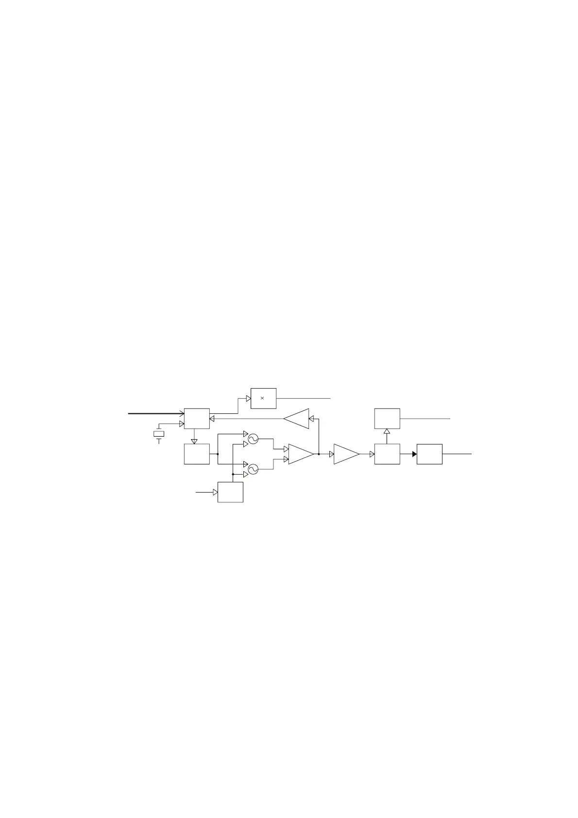
4-3 FREQUENCY SYNTHESIZER CIRCUITS
VCO
A VCO is an oscillator whose oscillating frequency is
determined by the applied volatge. This transceiver has two
VCOs; RX VCO and TX VCO. The RX VCO generates the
1st LO signals for the 1st IF signal produce, and TX VCO
generates TX signal.
• RX VCO (Q58, D38, 48)
The RX VCO oscillates 1st LO signals for normal RX
(174.350 to 183.325 MHz) and for WX channels (208.000–
209.625 MHz). The generated 1st LO signals are applied to
the 1st mixer (Q12) via the buffer AMPs (Q60 and Q28), LO
SW (D17) and the ATT.
• TX VCO (Q59, D45, 46)
The TX VCO oscillates 118.000–136.975 MHz transmit
signals. The generated TX signal is applied to the pre-driver
via buffers (Q60 and Q28), LO SW (D6) and ATT.
A portion of each VCO output is applied to the PLL IC via
the buffer (Q29).
PLL (Phase Locked Loop) CIRCUIT
The PLL circuit provides stable oscillation for both of the
TX and 1st LO frequencies (for RX). By comparing fedback
VCO output and reference frequency signals, the PLL
corrects the difference of these frequencies.
A portion of RX/TX VCO output is applied to the PLL IC via
buffer (Q29). The applied VCO output is divided according
to the serial data including divide ratio from the CPU, at the
prescaler and programmable divider. In the same way, the
reference frequency signal from the TCXO is applied to the
PLL IC and divided so that these two applied signals are
the same frequency.
The divided and frequency-matched signals (VCO output
and the reference frequency signals) are applied to the
phase comparator and phase-compared. The resulted
phase difference is detected as a phase-type signal, and
level-adjusted at the charge pump then output. The output
pulse type signal is passed through the loop filter to be
converted into the DC voltage (=Lock Voltage).
Applying the lock voltage to the variable capacitor which
composes a part of the resonator of RX/TX VCO, the
capacitance of variable capacitor changes corresponding
to the applied lock voltage. This causes the change of
resonation frequency that determines the VCO oscillating
frequency to keep the VCO frequency constant.
When the oscillation frequency drifts, its phase changes
from that of the reference frequency, causing a lock voltage
change to compensate for the drift in the VCO oscillating
frequency.
• FREQUENCY SYNTHESIZER CIRCUITS
PLL
IC
BUFFBUFF
FIL
LOOP
VCO
SW
BUFF
CR-783
X5
SHIFT
LO SW
154.350-183.325 MHz
118.000-136.975 MHz
D6,
Q28
Q60
Q29
RX VCO
TX VCO
Q58
D38,D48
Q59
Q57
R63,335,336
(15.300MHz)
IC29
RX-VCO
TX-VCO
PCK,PDATA,PSTB
(serial data)
ATT
D17
D45
3
(45.900MHz)
45.9MHz
2nd LO
1st LO signal
TX signal
Q84
208.000-209.625 MHz
R36-38
ATT
 Loading...