4 - 2
RX AF CIRCUITS
The RX AF circuits consist of AF fi lters, AF amplifi ers, etc.,
and amplify, fi lter the demodulated AF signals.
The demodulated AF signals from the IF IC are passed
through the AM/FM SW (IC2), and applied to the buffer
(IC18a). The AF bufffer-amplified AF signals are passed
through the 5-pole LPF (IC18b/c) to filter audio band signals
only, then buffer-amplified by another AF bufffer (IC18d).
The buffer-amplified AF signals are level-adjusted (audio
output level) by DAC (IC17_7), then applied to the AF power
AMP (IC31) via AF Pre-AMP (IC20). The AF signals are
power-amplified to obtain AF output level, then applied to
the internal speaker or external speaker via [SP] jack (J5).
SQUELCH CIRCUITS
The squelch circuit cuts off the AF output signals when no
RF signals are received.
• For receiving AM signals (RSSI SQUELCH)
The "RSSI" signal which is in proportion to the RX signal
level is applied to the CPU (IC26, pin 30). The CPU
interprets that RX signals are present or absent according
to the voltage of "RSSI" signal level.
• For recieving FM (WX) signals (NOISE SQUELCH)
A portion of FM demodulated AF signals is filtered by active
BPF (IC1; pins 12, 13, R790, 792, 793, C736, 737, 744)
which filters and amplifies only noise components (around
10 kHz signals) in the demodulated signals. The amplified
noise components are detected into pulse-type signal by
D79, then applied to the CPU (IC26) via the noise AMP
(IC28). The CPU interprets that RX signals are present or
absent by counting the pulse of noise signal.
If the CPU interprets that the RX signals are absent, the
CPU sends the "DETMUTE" signal to the AM/FM mute SW
(IC2). Then the AM/FM SW cuts off the AF line to close the
squelch.
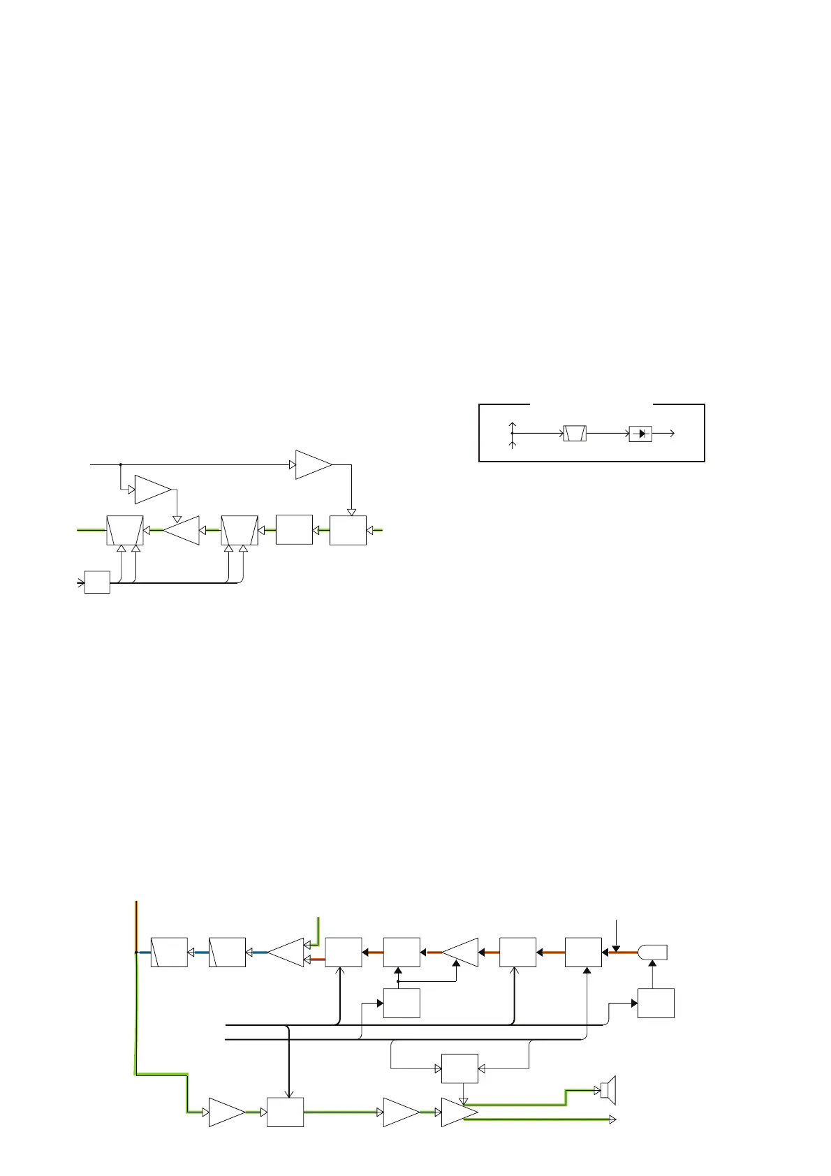
• AF CIRCUITS (for RX and TX)
MIC
MUT E
PWR
AMP
BUFF
LPFLPF
BUFF
From the ext. microphone
From the AM/FM SW (IC2)
MIC
AM P
PRE
AMP
To the ext. speaker
MMUT E
EMBI
ALCC
AFC
SPCON
MIC
CONTROL
AF AMP
CONTROL
ALC
CONTROL
To the int. speaker
(MIC VR)
DAC
IC17 _6
IC17 _5
IC17 _7
Q51
Microphone
MC1
D67
Q79
Q86
IC15
Q52
Q82,Q83,Q36
IC31
IC18a
IC18bIC18c
Control lines
from the CPU (IC26)
IC18d
DA2STB
SCK,SDATA
DA2STB
SCK,SDATA
DA2STB
SCK,SDATA
ALC
AM P
IC20
(MIC VR)
DAC
(VOLUME)
DAC
AGC (Automatic Gain Control) CIRCUITS
(For receiving AM signals)
The AGC circuit effectively reduces the RX signal level if
the signal is strong, and raises it when it is weaker. The
AGC circuit detects the overall strength of RX signals and
automatically adjusts the gain of RF and IF AMPs, and
attenuation level of the ATT to maintain an approximately
constant average level of the received signals (=the AF
output level).
• 2nd IF AMP gain control
The DC component in the AM-demodulated signals whose
signal level is in proportion to the RX signal (RF signal)
level, is fedback to the 2nd IF AMP in the IF IC. The DC
voltage controls the gain of 2nd IF AMP to keep the 2nd IF
signal level constant.
• RF AMP and 1st IF AMP gain control
The AGC voltage "RF AGC" which is in proportion to the RX
signal (RF signal) level is generated by the internal 2nd IF
AMP (similar as RSSI voltage). The AGC voltage “RF AGC”
is output pin 17 and applied to the AGC line drivers (Q10
and Q80) via AGC SW (Q85). Q10 controls the gain of RF
AMP (Q11), and Q80 controls the attenuation level of ATT
(D75–77) for stable 2nd IF signal level.
BPF
RF
AMP
BPF
AGC
AM P
AGC
AM P
ATT
T4
T3
T1
T2
D75
BEF
L52,C235
Q80
D13,50
Q10
Q11
D14,D15
L21,22
C67,71,73,326
IC17
DAC
RF AGC
RF AGC from IF IC
L18,69,
C60,327,780,781
• RF AMP AND 1ST IF AMP GAIN CONTROL
ANL (Automatic Noise Limiter) CIRCUIT
The ANL circuit is a limiter which reduces pulse-type noises
by cutting off the AF line temporarily. When the ANL function
is activated (ANL SW(Q21) is ON), demodulated AF signals
are applied to the cathode of D82 (switching diode) only. If a
pulse-type noise is included in the demodulated AF signals,
the cathode voltage of D82 becomes higher than that of
anode, and D82 turns OFF to cut-off the AF line. Thus, if the
RX signals contains pulse-type noise, the demodulated AF
signals are not applied to the AM/FM SW (IC2).
Fc=10 kHz
Active filter
From Pin16
Pin18 Pin13
To RX AF circuits
D79
Rectify
“NOISE”
NOISE SQUELCH DIAGRAM
 Loading...