5 - 3
LO
SW
D15,D16
Q7,D6,D7
MODULATION
FM:Analog
4FSK:Digital
D10
BUFF
Q15
BUFF
Q12
TX VCO
From the TX AF circuits
To the TX AMP circuits
MOD
LPF
PWR
DET
D27,D29,D35
MUTE
SW
Q23
ANT
SW
D24-D26,
D28,D32
PWR
AM P
IC3
APC
AMP
IC2
DRIVE
AMP
Q17
T1
TMUT
ANT
From the TX VCO
To the RX circuits
LPF
LPF
LO
SW
D15,D16
Q6,D4,D5
Q7,D6,D7
FILTER
LOOP
PLL
IC
SO,SCL,PLST
IC8
X3
Q4
Q19
To the TX AMPs
BPF
BUFF
Q15
BUFF
Q12
BUFF
Q11
X2
TCXO
LV
ADJ
D12
LV
ADJ
D11
ATT
IF IC
RX VCO
TX VCO
IC4
VCON
15.3MHz
45.9MHz
1st IF mixer
LV
LVA
Transmit circuits
Receive circuits
TX/RX common circuits
VCOs and LO buffers
AF power AMP
Logic circuits
CPU
+3
REG
Q1017,Q1019
+8
REG
IC1002
+5
REG
Q1014,Q1015
+3
REG
IC1001
W2
SW
POWER
Q1003
Q1001
T8
REG
Q1013,Q1016
R8
REG
+3.3V
RXC
CPU3.3V
R8V
VCC
PWON
8V
8V
VCC
8V
VCC
8V
+5V
TXC
8V
T8V
HV
VCC
D1008,Q1011,
Q1018,Q1021
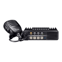
MODULATION CIRCUIT
The modulation signal from the TX AF circuits is applied to
D10 of the TX VCO (Q7, D6, D7, D10, D12) to modulate it
(FM for the analog mode, 4FSK for the digital mode). The
modulated signal from the TX VCO is buffer-amplified by
two buffers (Q12, Q15), and applied to the TX AMP circuits
through the LO SW (D15).
• MODULATION CIRCUITS
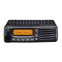
TX AMPLIFIERS
The buffer amplified signal from the LO SW (D15) is se-
quentially amplifi ed by the drive AMP (Q17) and power AMP
(IC3), to obtain TX power. The amplifi ed TX signal is passed
through the antenna SW (D24–D26, D28, D32) and the
LPFs, which eliminates harmonics, and then fed to the an-
tenna.
APC CIRCUITS
D27, D29 and D35 rectify a portion of the TX signal to direct
current, and the APC AMP (IC2) compares the voltage and
the TX power control reference voltage, “T1.” The resulting
voltage controls the gain of the power AMP (IC3) to keep the
TX power constant.
• TX AMPLIFIERS AND APC CIRCUITS
5-3
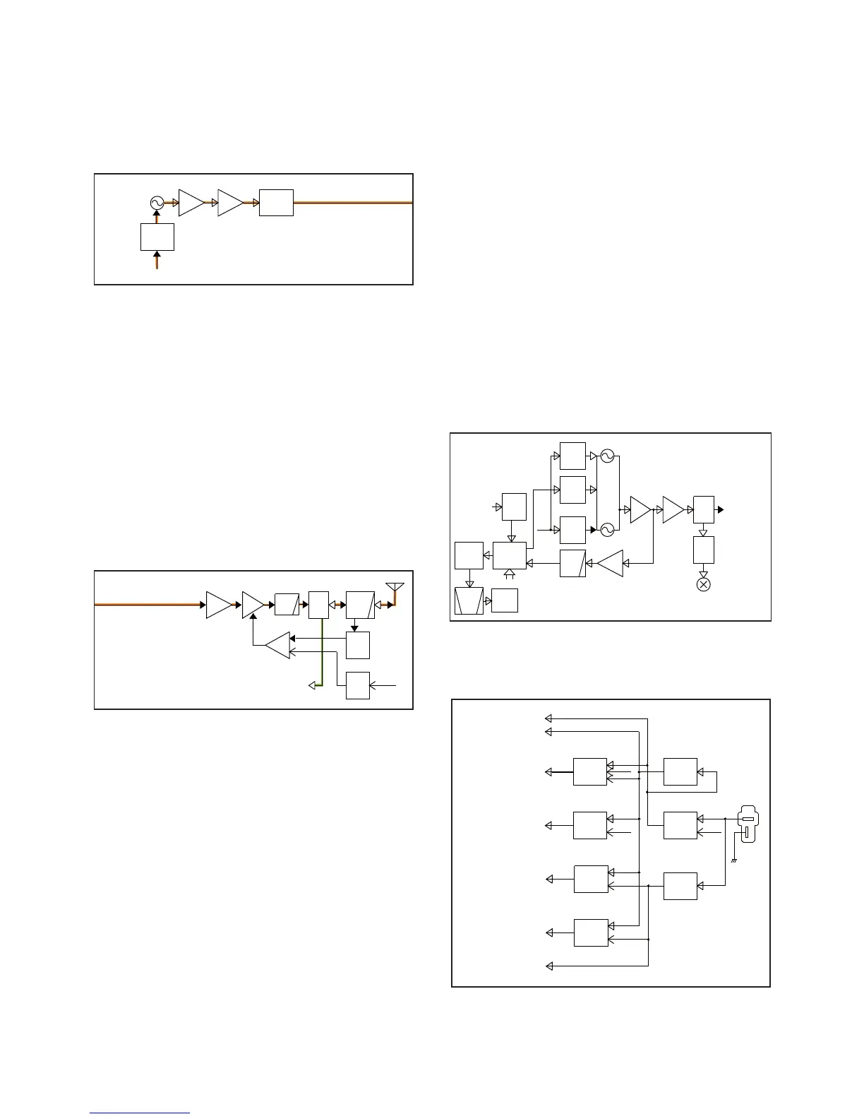
FREQUENCY SYNTHESIZER CIRCUITS
The RX VCO is composed of Q6, and D4, D5, D11. The
VCO output signal is buffer-amplified by two buffers (Q12
and Q15), and then applied to the 1st IF mixer, through the
LO SW (D16) and the attenuator.
The TX VCO is composed of Q7, D6, D7, D10 and D12. The
VCO output signal is buffer-amplified by two buffers (Q12
and Q15), and then applied to the drive AMP (Q17), through
the LO SW (D15) and the LPF.
A portion of signal generated by each VCO is fed back to the
PLL IC (IC8, pin 17) through the buffer (Q11) and the LPF
(L13, C298–C300).
The applied VCO output signal is divided and phase-com-
pared with a 15.3 MHz reference frequency signal from the
TCXO (X2), which is also divided. The resulting signal is
output from the PLL IC (IC8), and DC-converted by the loop
fi lter, and then applied to the VCO as the lock voltage.
When the oscillation frequency drifts, its phase changes
from that of the reference frequency, causing a lock voltage
change to compensate for the drift in the VCO oscillating fre-
quency.
• FREQUENCY SYNTHESIZER CIRCUITS
5-4 VOLTAGE DIAGRAMS
 Loading...