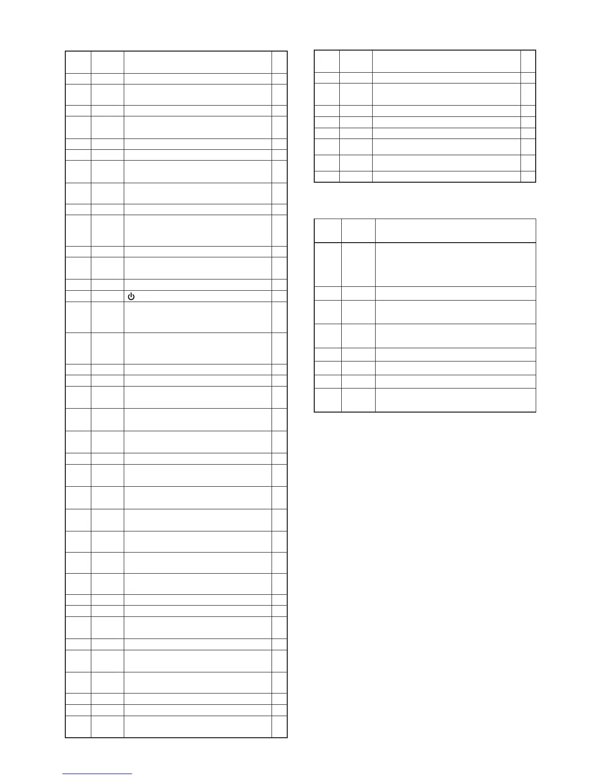
5 - 4
5-5 PORT ALLOCATIONS
• CPU (FRONT UNIT: IC51)
• D/A CONVERTER (IC1006)
PIN
No.
LINE
NAME
DESCRIPTION
23 T1
(TXPO)
During receiving: Outputs BPF tuning
voltage.
During transmitting: TX power reference
voltage.
24 T2 Outputs BPF tuning voltage
7 REF Outputs reference frequency adjust
voltage.
8 LVA Outputs additional lock voltage
adjustment.
11 SQLC Outputs Squelch threshold setting.
12 TENC Outputs CTCSS deviation adjustment.
19 BAL Outputs DTCS balance.
20 VRAF Outputs Max. deviation/AF volume
adjustment.
BALL
No.
LINE
NAME
DESCRIPTION
I/O
A1 KR1 [P1] input. I
A5 RXC
Power supply switching control.
H= During receive or stand-by.
O
A7 TDAT Serial data to the DSP (IC2007). O
A15 PWON
Power supply switching control.
H= The transceiver's power is ON.
O
B1 KR3 [P3] input. I
B2 KR0 [P0] input. I
B12 NOIS
Noise level detect.
H= Squelch close
I
B13 EPTT
External PTT input.
H= An external PTT is pushed.
I
B14 PGIO4 External I/O port. I/O
B15 AFON
AF mute SW control.
H= During the squelch circuit is
activated.
O
C3 KR2 [P2] input. I
C5 TXC
Power supply switching control.
H= While transmitting.
O
C8 ESDA EEPROM (IC52) serial data. I/O
C13 POSW [
] input. I
C14 ADS
1st IF filters (FI4 and FI5) switching
control.
L= During digital mode.
O
C15 NWC
Receive mode (narrow/mid/wide)
switching.
L= During narrow mode.
O
D6 DSCK DSP (IC2007) clock. O
D8 ESCL EEPROM (IC52) clock. O
D13 DPDN
DSP (IC2007) power control.
H= DSP is inactivated
O
D14 DRES
DSP (IC2007) reset.
L= Reset
O
D15 CSFT
Clock frequency shift.
H= Clock frequency is shifted.
O
E13 CRES CPU reset. I
H1 SIDE1
[
Y
] key input.
L= Pushed
I
H2 SIDE2
[
Z
] key input.
L= Pushed
I
J1 IPTT
Microphone [PTT] input.
L= Pushed.
I
K3 LIGT1
LCD dimmer control.
H= Dimmer OFF.
O
L1, L2
MCG0,
MCG1
MIC gain control. O
L3 LIGT2
Backlight control.
H= Backlight ON.
O
L14 SSO Common serial data. O
L15 SCK Common clock. O
M1 TMUT
Transmission mute.
L= TX inhibit.
O
M8 BEEP Beep audio. (Square waves) O
M14 DAST
D/A converter (IC1006) strobe.
H= Load enable.
O
N2 LINH
LCD driver (IC6) chip enable.
H= Enable.
O
N12 BATV Power supply voltage sensing. I
N14 RDAT DSP (IC2007) serial data. O
N15 IGSW
Ignition SW detect.
L=Ignition detected.
I
BALL
No.
LINE
NAME
DESCRIPTION
I/O
P2 LCS LCD driver (IC6) chip O
P4 PLSW
PLL lock up time control.
L= Fast lock up
O
P10 TEMP Temperature sensing voltage. I
P11 RSSI RSSI sensing voltage. I
P12 AFVI [VOLUME CONTROL] input. I
R1 LSO LCD driver (IC6) serial data. O
R4 PLST PLL strobe. O
R10 LVIN Lock voltage input. I
 Loading...