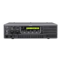
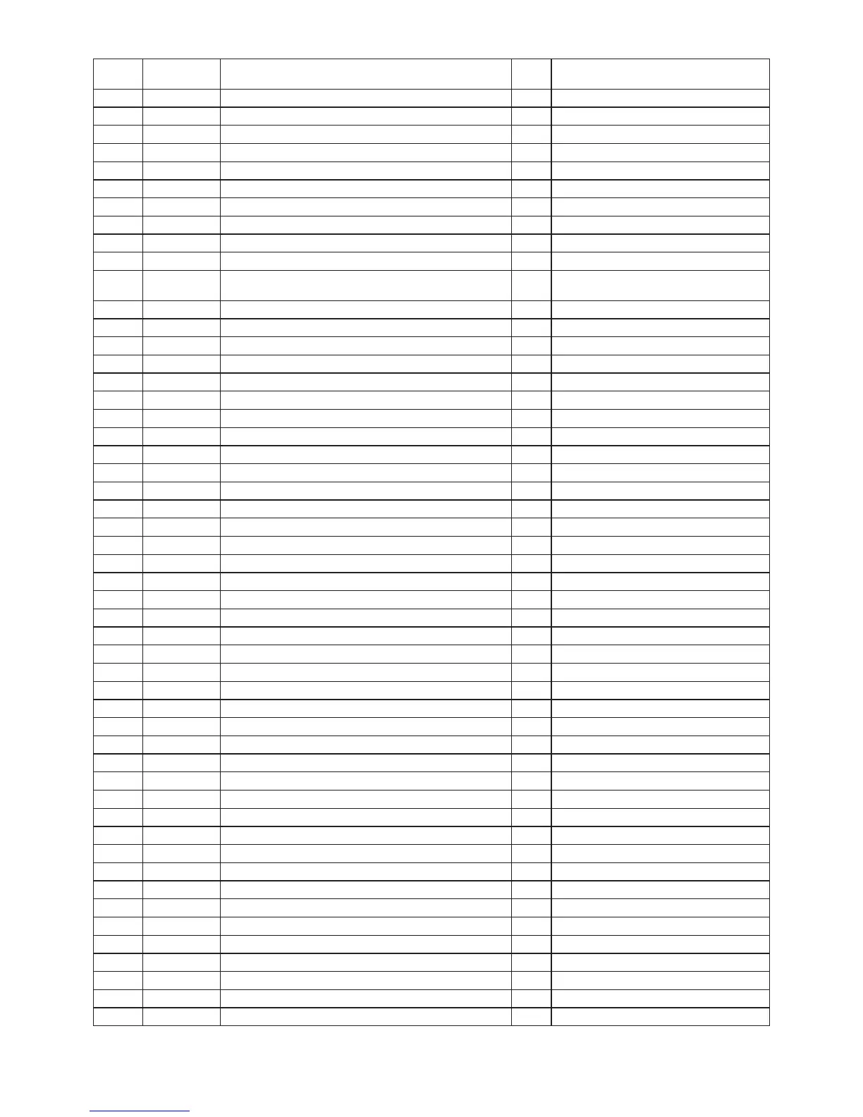
5 - 3
Pin
No.
LINE NAME DESCRIPTION
IN/
OUT
CONDITION
1–11 D5–D15 DSP data bus line. I/O –
15–28 A1–A14 DSP data bus line. I/O –
29 HRW DSP data line. I/O –
32 FANS Cooling fan (CH: MF1) rotation detect. I "H"=While the cooling fan is rotating.
33 TLED TX indicator LED control signal. O "H"=TX
34 LEDR RX indicator LED control signal. O "H"=Squelch open.
35 PLSCK PLL (M: IC4) serial clock. O –
36 PLSSO PLL (M:IC4) serial data. O –
41 PWON Power line "VCC" control signal. O "H"=Power ON.
42 AFON2 AF power AMP. (M: IC28) control signal. O "H"=AF power AMP ON.
43 AFON AF output select signal. O
"H= AF signals are output from the
[ACCESSORY CONNECTOR].
44 ESCL Serial clock to the EEPROM (M: IC21). O –
45 ESDA Serial data to the EEPROM (M: IC21). O –
46 TXC TX power line "T8V" control signal. O "H"=TX
47 RXC RX power line "R8V" control signal. O "H"=RX
48 RPLST RX PLL (M: IC4) strobe. O –
49 TPLST TX PLL (M: IC3) strobe. O –
50 RUNLK RX PLL (M: IC4) unlock signal. I "L"=Unlocked
51 TUNLK TX PLL (M: IC3) unlock signal. I "L"=Unlocked
52 XCTS Serial data from the RS-232 line driver (M: IC26). I –
53 XRTS Serial data to the RS-232 line driver (M: IC26). O –
55 EXDA External D/A port. O –
56 BEEP Beep sounds (square waves). O –
57–59 OPV3–OPV1 Optional unit detect. I –
60 MMUT MIC mute signal to the installed optional unit. O "H"=MIC mute
61 HANG Microphone hang-up detect. I "L"=Hang-up
62 PTT [PTT] key input. (pull up) I –
63 RMUT RX mute signal to the installed optional unit. O "H"=RX mute
64 EXAD External A/D port. I –
65 TEMP Temperature detect. I –
68 RLVIN RX PLL lock voltage. I –
69 BATV Voltage monitor (divided voltage of "VCC"). I –
70 TLVIN TX PLL lock voltage. I –
71 RSSI RSSI signal from the IF IC (M: 5). I –
74 XTXD External data to the RS-232 driver (M: IC26). O –
75 XRXD External data from the RS-232 driver (M: IC26). I –
76 TMUT TX mute signal. O "H"=TX mute
77 HINT DSP IC control signal. O –
78 INT1 DSP IC control signal. O –
79 HRDY DSP IC control signal. O –
81 HDS1 DSP IC control signal. O –
82 HDS2 DSP IC control signal. O –
100 RES CPU reset signal from the reset IC (F: IC501). O –
101–108 EXIO1–EXIO8 External data bus line. I/O +5 V pull-up
112 POSW [PWR] key input. (pull-up) I –
113 NOIS Noise detect. I "H"=RX signal is absent (squelch close).
114 CSFT Clock frequency shift signal. O –
119 SSO Serial data to the seri-para converter (M: IC31). O –
120 SCK Clock signal to the seri-para converter (M: IC31). O –
121 EXIO9 External data bus line. I/O +5 V pull-up
122 DSDA Serial data to the DAC (M: IC17). O –
5-5 CPU (M: IC20) PORT ALLOCATION
 Loading...