4 - 4
4-2-5 APC CIRCUIT (MAIN UNIT)
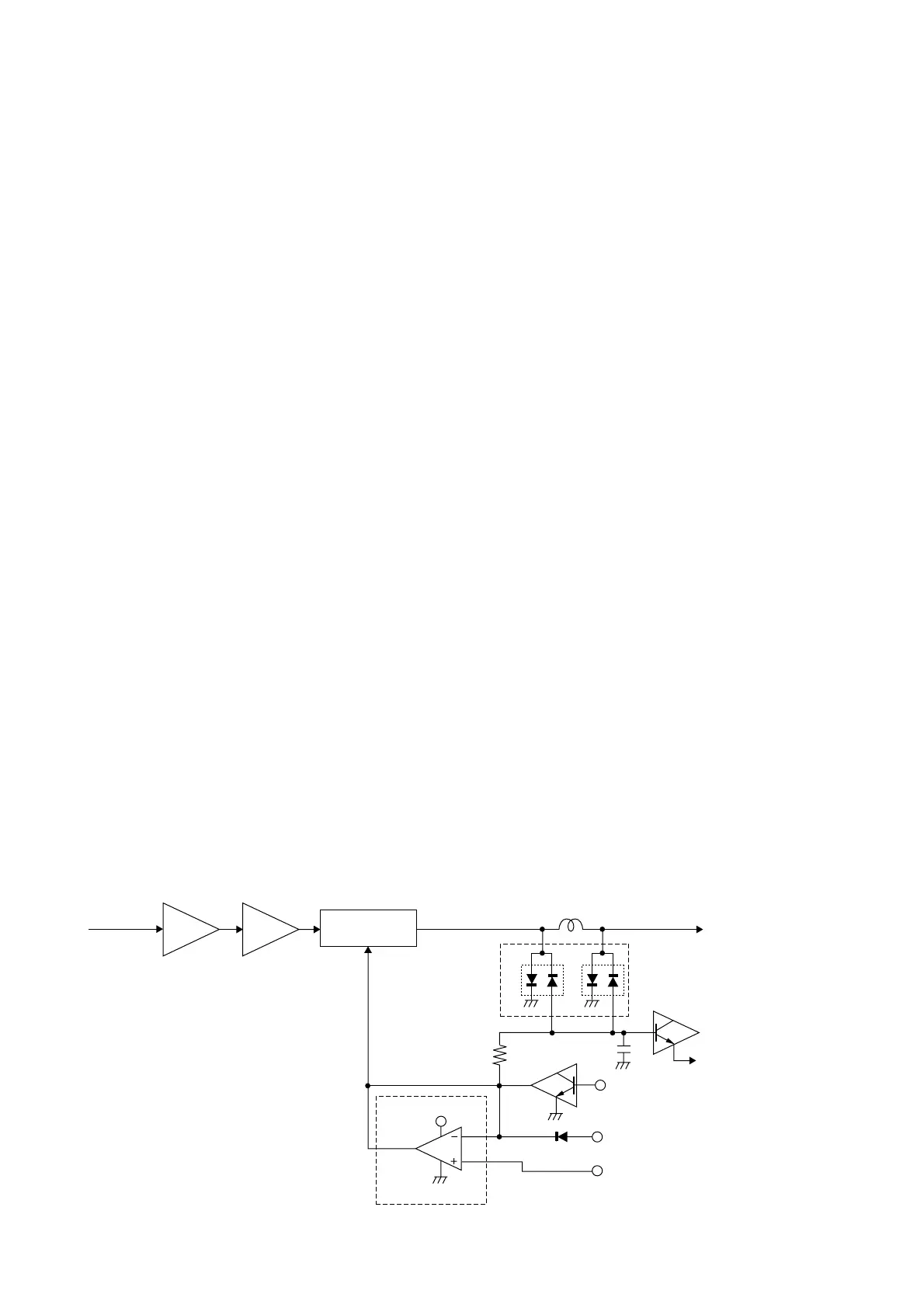
The APC (Automatic Power Controller) circuit stabilizes the
TX output power.
The RF output signal from the power amplifier (IC13) is
detected at the power detector circuit (D47, D48) and is
applied to APC controller. The applied voltage compares to
“PCON” signal from the D/A converter IC (IC15, pin 14), and
then outputs the differential bias voltage for power amplifier
(IC13, pin 3). Thus the APC circuit maintains a constant out-
put power.
4-3 PLL CIRCUITS
4-3-1 GENERAL
The PLL circuit provides stable oscillation of the transmit fre-
quency and receive 1st LO frequency. The PLL circuit com-
pares the phase of divided VCO frequency with the refer-
ence frequency. The PLL output frequency is controlled by
the crystal oscillator and divided ratio of the programmable
divider.
IC12 is a dual PLL IC, which controls both TX and RX VCO
circuits, and contains a prescaler, programmable counter,
programmable divider, phase detector, charge pomp and
etc.
The PLL circuit, using a one chip PLL IC (IC12), directly gen-
erates the transmit frequency and receive 1st IF frequency
with VCOs. The PLL IC sets the divided ratio based on ser-
ial data from the main CPU, and compares the phases of
VCO signals with the reference oscillator frequency. The
PLL IC detects the out-of-step phase and outputs from pins
8 and 13 for TX and RX, respectively. The reference fre-
quency (15.3 MHz) is oscillated at the reference oscillator
(X4).
4-3-2 TX AND CHANNEL 70 (RX) LOOPS
The generated signal at the TX-VCO/CHANNEL 70-VCO
(Q18, D39, D40) enters the PLL IC (IC2, pin 2) and is divid-
ed at the programmable divider section and is then applied
to the phase detector section.
The phase detector compares the input signal with a refer-
ence frequency, and then outputs the out-of-phase signal
(pulse-type signal) from pin 8.
The pulse-type signal is converted into DC voltage (lock
voltage) at the loop filter (R217–R219, C247, C249, C278),
and is then applied to the varactor diodes (D39, D40) of the
TX-VCO to stabilize the oscillated frequency.
4-3-3 OTHER CHANNELS (RX) LOOP
The generated signal at the RX-VCO (Q12, D32, D33)
enters the PLL IC (IC2, pin 19) and is divided at the pro-
grammable divider section and is then applied to the phase
detector section.
The phase detector compares the input signal with a refer-
ence frequency, and then outputs the out-of-phase signal
(pulse-type signal) from pin 13.
The pulse-type signal is converted into DC voltage (lock
voltage) at the loop filter (R182, R213, R214, C225, C248),
and is then applied to the varactor diodes (D32, D33) of the
RX-VCO to stabilize the oscillated frequency. The lock volt-
age from the loop filter is amplified at the buffer amplifier
(Q23), and is then applied to the RF circuit.
 Loading...