3 - 5
3-2-8 APC CIRCUIT
The APC (Auto Power Control) circuit protects the power
amplifiers on the PA unit from high SWR and excessive
current.
(1) SWR APC (FILTER BOARD AND MAIN UNIT)
The reflected wave signal appears and increases on the
antenna connector. When the antenna is mismatched,
D4310 of the power detector circuit (FILTER board; D4309,
D4310, L4341) detects the signal and applies it to the APC
amplifier (MAIN unit; Q23). The amplified signal decreases
the bias voltage of the RF ALC amplifier to reduce the out-
put power.
(2) CURRENT APC (PA150W BOARD AND MAIN UNIT)
The power transistor current is detected from the differ-
ent voltages between both terminals of a 0.012 Ω resistor
(R4026) on the PA150W board. The detected voltage is
applied to the differential amplifier (IC4002b). When the cur-
rent of the final transistors is more than 30 A, the detected
voltage is applied to the APC amplifier controller (MAIN
unit; Q111) to reduce the gate-2 voltage of the IF amplifier
(MAIN unit; Q2) and thus reduce the output power.
3-2-9 TEMPERATURE DETECTION
(PA150W BOARD)
Thermal switches (S4001, S4002) protect the final transis-
tors from excessive temperatures. When the temperature of
the final transistors exceeds 50˚C (122˚F), S4002 is turned
ON to start the cooling fan. When the temperature of the
final transistors exceeds 110˚C (230˚F), S4001 is turned
ON to control the “POC2” line and sets the power to 60 W.
3-2-10 RF METER CIRCUIT (MAIN UNIT)
The output of the ALC amplifier (IC16a) is applied to the
CPU (pin 31) to indicate the transmit power level on the
display.
For antenna current meter indication, the “ANTC” signal
from an optional AT-130E is applied to the CPU (pin 32).
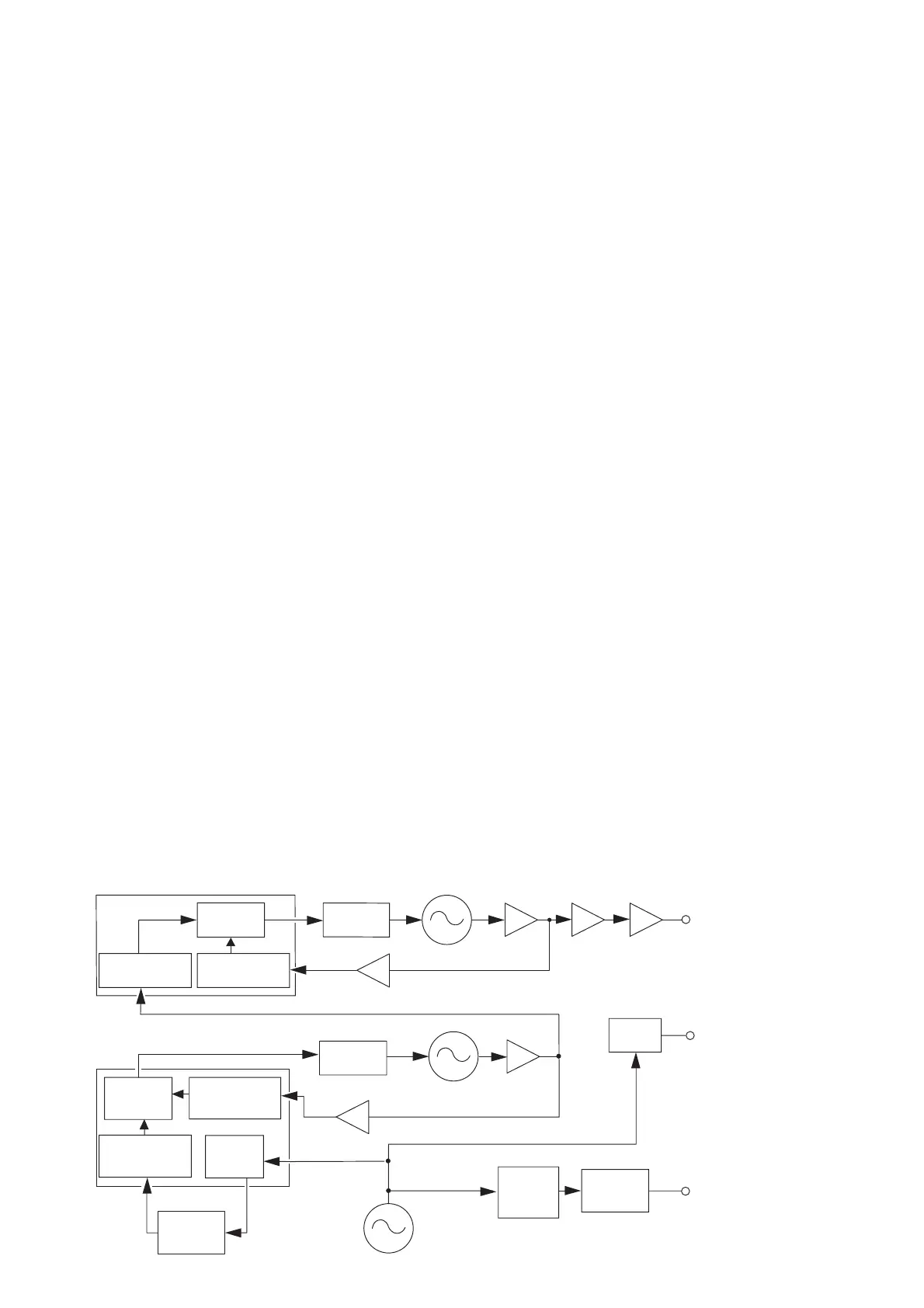
3-3 PLL CIRCUIT
3-3-1 GENERAL
The PLL unit generates a 1st LO frequency (69.5115–
99.0114 MHz), 2nd LO frequency (60 MHz) and a BFO fre-
quency (9.0106–9.013 MHz) for the MAIN unit. The 1st LO
PLL adopts a mixerless dual loop PLL system. The BFO
uses a DDS and a 2nd LO as a fixed frequency double that
the crystal oscillator.
3-3-2 1ST LO PLL (PLL UNIT)
The 1st LO PLL contains a main loop and reference loop
as a dual loop system. The reference loop generates a
10.65 to 10.75 MHz frequency using a DDS circuit, and the
main loop generates a 69.5115 to 99.0114 MHz frequency
using the reference loop frequency.
(1) REFERENCE LOOP PLL
The oscillated signal at the reference VCO (Q3005, D3003)
is amplified at the buffer amplifiers (Q3006, Q3011) and is
then applied to the DDS IC (IC3001, pin 46). The signal is
then divided and detected on phase with the DDS gener-
ated frequency.
The detected signal output from IC3001 (pin 56) is convert-
ed into a DC voltage (lock voltage) at the loop filter (R3018,
R3019, C3044) and then fed back to the varactor diode
(D3003) in the VCO circuit.
(2) MAIN LOOP PLL
The oscillated signal at the main loop VCO (Q3003, D3004)
is amplified at the buffer amplifiers (Q3004, Q3008), and is
then applied to the PLL IC (IC3005, pin 14). The signal is
then divided and detected on phase with the reference loop
output frequency.
The detected signal output from IC3005 (pins 3009, 3010)
is converted into a DC voltage (lock voltage) at the loop
filter and then fed back to the varactor diode (D3004) in the
VCO circuit.
The oscillated signal is amplified at the buffer amplifiers
(Q3004, Q3021, Q3024) and then applied to the MAIN unit
as a 1st LO signal.
PLL IC (IC3005)
Programmable
divider
Programmable
divider
Programmable
divider
Programmable
divider
Phase
Phase
detector
detector
DDS
D/A
convertor
convertor
Loop filter
Loop filter
Q3011
Reference loop VCO
Q3005/D3003
Q3008
Main loop VCO
Q3004
Q3003/D3004
10.65–10.75 MHz
Q3006
DDS
IC3002
Q3002
Doubler
D/A
Reference OSC
X3001; 30.0 MHz
Q3021 Q3024
1LO
(69.5115–99.0114 MHz)
2LO
(60.0 MHz)
BFO
(9.0106–9.013 MHz)
DDS IC
(IC3001)
• PLL CIRCUIT
 Loading...