3 - 6
3-3-3 2ND LO AND REFERENCE OSCILLATOR
CIRCUITS
The reference oscillator (X3001) generates 30.0 MHz fre-
quency used for the both DDS ICs as a system clock and
for the LO output. The oscillated signal is doubled at the
driver (Q3002) and picked up the 60 MHz frequency at
the resonator circuit (L3004, L3005). The 60 MHz signal is
applied to the MAIN unit as a 2nd LO signal.
3-3-4 BFO CIRCUIT
The DDS IC (IC3002) generates a 10-bit digital signal
using the 30 MHz system clock. The digital signal is con-
verted to an analog wave signal at the D/A converter (R3120
–R3139). The analog wave is passed through the low-pass
filter (L3037, L3038, C3154–C3158), and is then applied
to the MAIN unit as the BFO signal. The PA unit separate
grounding from the other units to obtain floating.
3-4 DC-DC converter CIRCUIT
(REG UNIT; [EUR] only)
The IC-M710 [EUR] version employs a floating ground-
ing system which is not connected between transceiver’s
ground and (–) terminal of the power supply. The PA unit
separate grounding from the other units to obtain floating.
The 13.6 V DC from the DC power connector passes
through the noise filter (L8001, C8001–C8005), and is then
applied to the switching transformer (T8001). The MOS
FET (Q8001) is turned ON and OFF by D8003 and Q8003
respectively.
IC8001 is a switching control IC which contains a 5 V refer-
ence voltage regulator (pins 12, 14), two error amplifiers
(pins 1–3, 15, 16), a saw tooth oscillator (pins 4–6) and
a comparator. The switching frequency is determined by
R8008 and C8007 and is set at 36 kHz.
AC voltage appear on the secondary terminals of T8001
and rectified by D8002. The rectified DC voltages are
passed through the noise filter (L8003, C8009, C8010),
and are then applied to the MAIN unit as a 13.6 V DC volt-
age line.
1
10
11
16
17
18
20
21
22
23
24
25
26
27
28
30
31
32
33
34
35
36
Input port for the CPU reset signal.
When receiving a “LOW” pulse, the
CPU is reset.
Data input port from the sub CPU in
the FRONT unit.
Data output port to the sub CPU in
the FRONT unit.
Input port to the sub CPU in the
FRONT unit.
Outputs low power control signal for
60 W power.
Outputs low power control signal for
20 W power.
Input port for the CW keying.
High: When key is closed.
Outputs a “SEND” control signal for
the ACC (1) and ACC (2) sockets.
Outputs a “SEND” control signal for
T8 and R8 voltage line control.
Low : For transmit.
Outputs an alarm control signal to
activate the 2-tone emergency alarm
encoder.
High : Alarm ON.
Outputs a tone switching signal for the
2-tone emergency alarm encoder.
High : High tone.
Outputs a clock signal for the
EEPROM (IC134).
Data bus line for the EEPROM
(IC134).
Outputs a serial signal for the
EEPROM (IC135).
Data bus line for the EEPROM
(IC135).
Input port for the S-meter indication.
Input port for the RF-meter indication.
Input port for the antenna current
meter indication for [EUR] version.
The ANTC signal can be received
when an optional AT-130E is con-
nected.
Input port for the squelch detected
signal.
High : When squelch is open.
Input port for the transmit/receive
switching signal.
Input port for the scan control signal
from the ACC (1) socket.
Outputs RF gain control signal to the
AGC circuit.
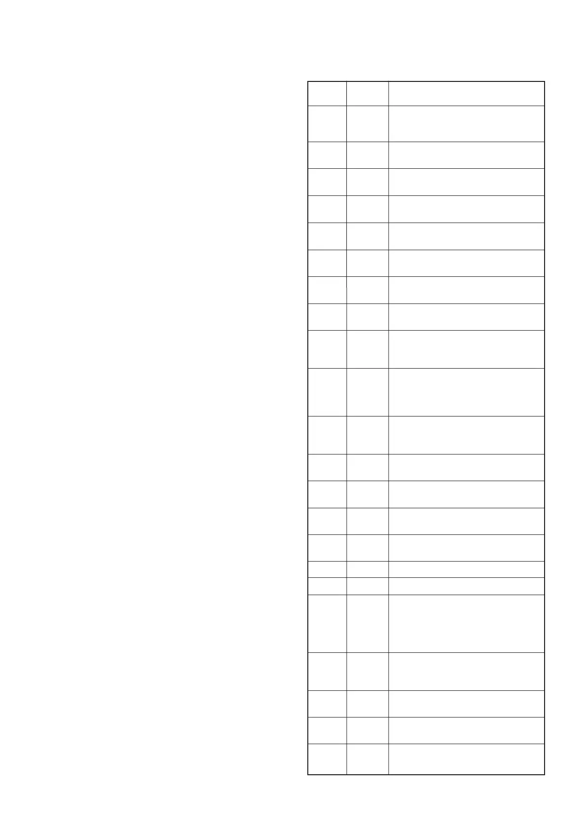
3-5 PORT ALLOCATIONS
CPU (MAIN unit; IC132)
RES
RXDO
TXDO
NSEN
POC2
POC1
CWIN
ASEN
CSEN
ALMS
ALMC
SCL
SDA
SO
SDA
RSM
MFOR
ANTC
SQLS
TRC
SCAS
RFG
Pin Port
Description
number name

 Loading...