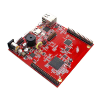
User Manual 3-2 V2.0
Application Kit TC3X7 ADAS V2.0 2018-06
Application Kit Manual TC3X7 ADAS
Hardware: Application Kit TC3X7 ADAS V2.0
Application Kit Information
– Configurable window watchdog
– Configurable functional watchdog (not with TLF30682QVS01)
– Microcontroller monitoring via ERR pin (not with TLF30682QVS01)
– Green Product (RoHS compliant)
– ISO26262 compliant up to ASIL D (not with TLF30682QVS01)
–AEC Qualified
The TLF3068x is connected to the CPU via QSPI2 and use QSPI2_SLSO1 (P14.2) as chip select. Via this spi
connection the power supply will be configured (Watchdog, device states and soon).
For more information see the data sheet of TLF3068x.
Note: The switch to FAILSAFE state is switched off by HW (R127 assembled). If you will use/evaluate all safety
features of the TLF3068X make sure that R127 is not assembled and remove R127 if assembled. Make
sure that you have a proper initialization of TLF3068X in your software and debugger in this case. If
needed you can assemble JP201 (2 pin header). Then you can switch easily with a jumper
3.3 Real Time Clock
The board is equipped with a RTC MCP79511 (if I2C is not supported by CPU) or MCP79411 (if I2C is supported by
CPU) from Microchip. The device is powered from the processor voltage of the TLF3068x (+3,3V). For backup when
the TLF3068x is not powered or switched off then there is a small battery to hold the value inside the RTC. The
MCP79511 is connected to the microcontroller via QSPI4, the MCP79411 is connected to the microcontroller via
I2C on P15.4/P15.5. The RTC can trigger an SCU_REQ4 (P33.7) interrupt (activ low) with the alarms. Also an alarm
from the RTC will wake-up (switch on) the board if the board is powered and the supply is switched off.
The MCP79511/MCP79411 contains also an unique ID in the format EUI-48. This id can be used as mac id for
ethernet if the assembled CPU support ethernet.
For more information about the RTC please see the datasheet of MCP79511/MCP79411.
3.4 XGA Display
The board has an XGA Display with a resolution of 320x240. The display has an ILI9341 display controller. Please
see the datasheet of the display controller for the register of the controller. The display is connected to the the
microcontroller via an SPI to Parallel converter (U201).
The SPI to Parallel converter is based on a statemachine. This state machine is clocked with the clock of SPI, here
SCLK0 (P20.13). Each rising edge of P20.13 will change the state of statemachine. When SLSO08 (P20.6) is not low
then the state machine will go always in the idle state with a valid clock edge.
The backgound light is switched on via port 15 pin 0. An high level on this port pin enable the backgound light.
3.4.1 Write a display register
A single write to any register can be done by a 32 bit transfer of SPI. Make sure that the SLSO08 is low during this
32 bit. Bit 31 must be transfered first.
Bit 31 must be 0, this will be indicate a write access.
Bit 30 must be 0, this will be indicate a single access.
Bit 29...Bit 22 is the 8 bit register number which will be written
Bit 21...Bit 6 is the 16bit value which will be written
Bit 5...Bit 0 are dummy bits which are used to execute the write.
To speedup the writing (e.g. write to ram of display controller) it is possible to make a endless transfer. This is
done by this:

 Loading...