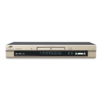
XV-SA600BK/XV-SA602SL
45
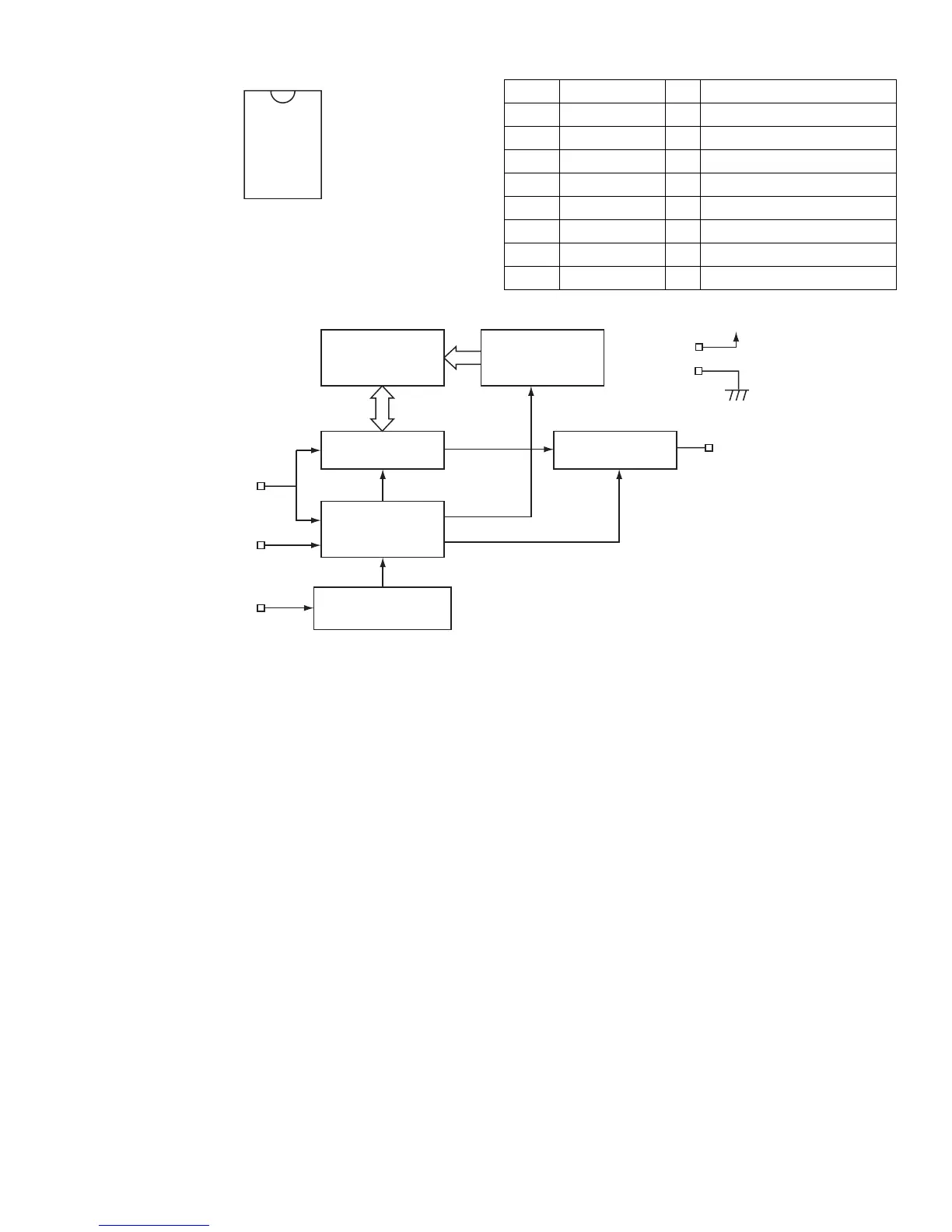
4.13 S-93C66AFJ-X (IC451,IC510) : EEPROM
4.13.1 Pin layout 4.13.2 Pin function
4.13.3 Block diagram
1
2
3
4
8
7
6
5
PE
CC
CS
SK
NC
GN
DO
DI
Pin No. Symbol I/O Description
1 PE - Non connect
2 VCC - Power supply terminal
3 CS I Chip select input
4 SK I Serial clock input
5 DI I Serial data input
6 DO O Serial data output
7 GND - Connect to ground
8 NC - Non connect
DI
S
K
DO
Vcc
GND
Memory
array
Address
decoder
Data resister
Mode decode
logitech
Clock generation
circuit
Buffer output
 Loading...