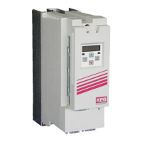
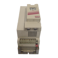
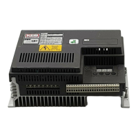
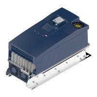
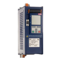
7 Connection of the Control
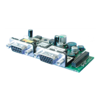
7.1 Control board for F5 AIC devices
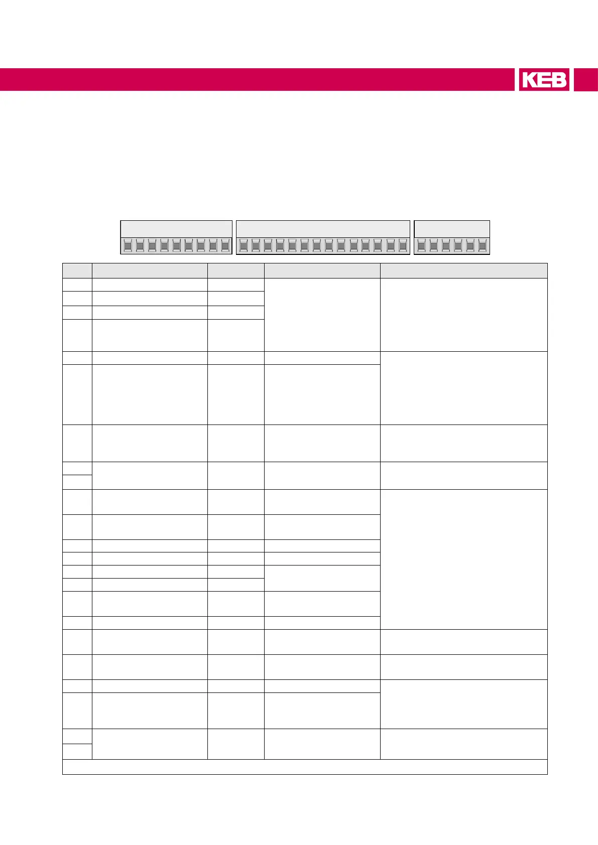
7.1.1 Assignment of the terminal block X2A
123456789
10 11 12 13 14 15 16 17 18 19 20 21
22 23 24 25 26 27 28 29
PIN Function Name Default assignment Description
1 + Setpoint input 1 AN1+ The input signal 0...±10V; 0...±20mA
and
4...20mA is determined with An.00
/ An.10. Resolution: 12 Bit, Ri =
30kΩ,scantime:1ms/atfastset-
pointsetting:250μs
2 - Setpoint input 1 AN1-
3 + Setpoint input 2 AN2+
4 - Setpoint input 2 AN2-
5 Analog output 1 ANOUT1 The output at the analog output
is set with An.31 / An.36. Voltage
range:0...±10V,Ri=100Ω,res-
olution: 10 Bit, PWM frequency:
3.4kHz,limitingfrequencylter1.
Order: 178Hz
6 Analog output 2 ANOUT2
7 +10 V output CRF Reference voltage output +10V DC
+5% / max. 4mA for setpoint poten-
tiometer
8
Analog ground COM
Ground for analog inputs and out-
puts
9
10 Progr. input 1 I1
2. Setpoint of the control
voltage
All digital inputs are freely program-
mable.Thecontrolreleaseisrmly
linked with the input ST, but can be
assigned with additional functions.
Ri=2.1kΩ
Scan time: 1ms
11 Progr. input 2 I2
Switch-on delay, control
release ST
12 Progr. input 3 I3
13 Progr. input 4 I4
14 Progr. input forward F
15 Progr. input reverse R
16
Progr. input control
release
ST ST
17 Progr. input reset RST RST
18 Transistor output 1 O1 Control main contactor
(DC > level)
Max. 50mA DC for both outputs are
available.
19 Transistor output 2 O2 Ready for operation (Uic
loaded)
20 +24 V output U
out approx. 24V DC output (max.
100mA), voltage input for ext.
supply, reference potential 0V
X2A.22/23
21 20...30 V input U
in
22
Digital ground 0V
Reference potential for digital in-
puts/outputs
23
continued on the next page
49
CONNECTION OF THE CONTROL
 Loading...