TK-3170/3173
23
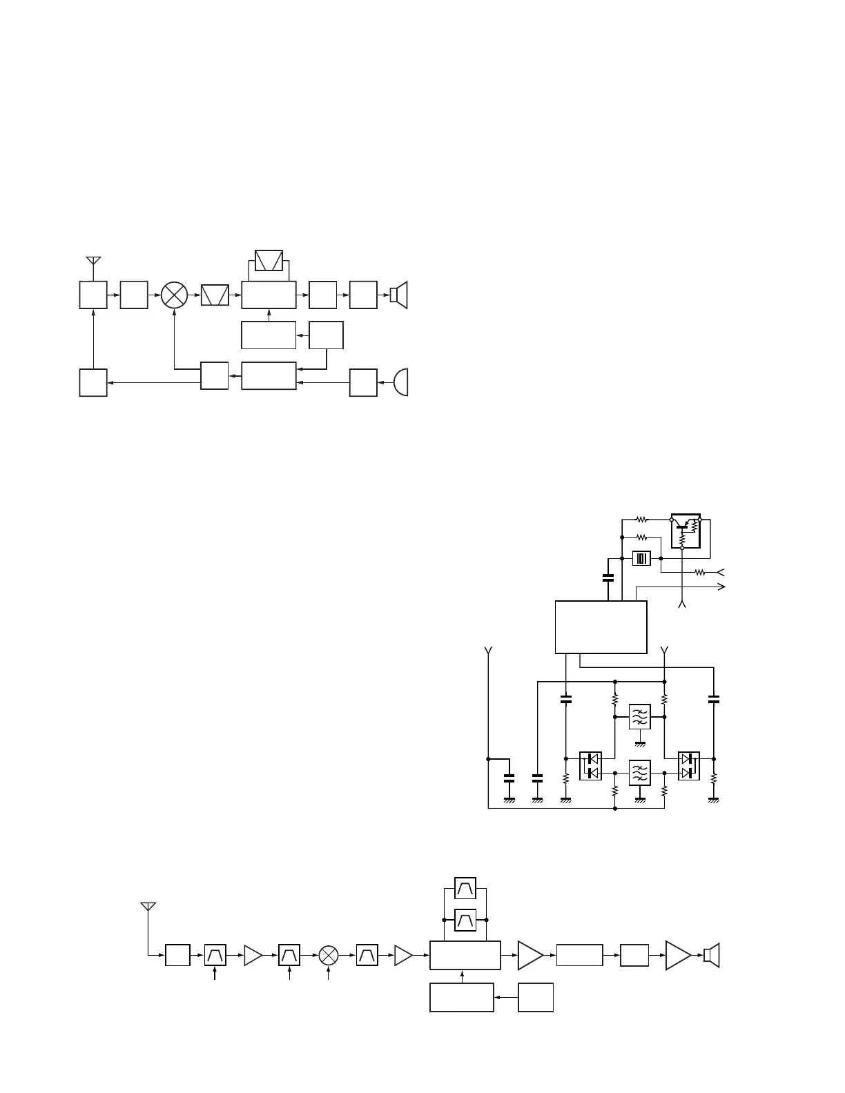
1. Frequency Configuration
The receiver utilizes double conversion. The first IF is
49.95MHz and the second IF is 450kHz. The first local oscil-
lator signal is supplied from the PLL circuit.
The PLL circuit in the transmitter generates the necessary
frequencies. Figure 1 shows the frequencies.
crystal filter (XF701) to remove the adjacent channel signal.
The filtered first IF signal is amplified by the first IF amplifier
(Q703) and then applied to the lF system IC (IC701). The IF
system IC provides a second mixer, second local oscillator,
limiting amplifier, quadrature detector and RSSI (Received
Signal Strength Indicator). The second mixer mixes the first
IF signal with the 50.4MHz of the second local oscillator out-
put (TCXO X501) and produces the second IF signal of
450kHz.
The second IF signal is passed through the ceramic filter
(Wide : CF701, Narrow : CF702) to remove the adjacent chan-
nel signal. The filtered second IF signal is amplified by the
limiting amplifier and demodulated by the quadrature detec-
tor with the ceramic discriminator (CD701). The demodu-
lated signal is routed to the audio circuit.
2-4. Wide/Narrow Switching Circuit
Wide and Narrow settings can be made for each channel
by switching the ceramic filters CF701 (Wide), CF702 (Nar-
row). The Wide and Narrow is output from IC4.
D701 and D702 are switched to ceramic filters when a
Wide/Narrow level is selected.
Q702 turns on/off with the Narrow and the IC701 detector
output level is changed to maintain a constant output level
during wide or narrow signals.
CIRCUIT DESCRIPTION
ANT
TX/RX : 450~490MHz (K,K4)
440~480MHz (M)
400~430MHz (K,K6,M3)
450~490MHz (K,K4)
440~480MHz (M)
400~430MHz (K,K6,M3)
ANT
SW
RF
AMP
TX
AMP
1st MIX
MCF
49.95MHz
CF
450kHz
IF
SYSTEM
AF
AMP
SP
50.4MHz
400.05~440.05MHz (K,K4)
390.05~430.05MHz (M)
350.05~380.05MHz (K3,K6,M3)
PLL
VCO
MIC
AMP
MIC
X3
multiply
TCXO
16.8MHz
RF
AMP
VOL
q
q
Fig. 1 Frequency configuration
2. Receiver System
The receiver system is shown in Figure 2.
2-1. Front End (RF AMP) Circuit
The signal coming from the antenna passes through the
transmit/receive switching diode circuit (D604, D605, D606
and D608), passes through a BPF (L717 and L718), and is
amplified by the RF amplifier (Q705).
The resulting signal passes through a BPF (L711, L712 and
L713) and goes to the mixer. These BPFs are adjusted by
variable capacitors (D703, D704, D705, D706 and D707). The
input voltage to the variable capacitor is regulated by voltage
output from the DC amplifier (IC19).
2-2. First Mixer
The signal from the front end is mixed with the first local
oscillator signal generated in the PLL circuit by Q704 to pro-
duce a first IF frequency of 49.95 MHz.
The resulting signal passes through the XF701 MCF to cut
the adjacent spurious and provide the optimum characteris-
tics, such as adjacent frequency selectivity.
2-3. IF Amplifier Circuit
The first IF signal is passed through a four-pole monolithic
MXO
AFOUT
QUAD
IFOUT
IFI
Wide
C702
C701
C708
C719
R705
R702
R701
R703
R706
C709
R708
D702 D701
CF701
CF702
IC701
R719
R717
Q702
R718
5C
AFOUT
Narrow
Narrow
CD701
Fig. 2 Receiver system
Fig. 3 Wide/Narrow switching circuit
IC701
IF, MIX, DET
AQUA-L
ANT
SW
BPF
Q705
RF
AMP
Q704
1st MIX
Q703
IF AMP
ANT
BPF
XF701
MCF
1st Local
TUNE TUNE
CF702
CF701
SP
Q701
X3 multiply
2nd Local
IC10
AF AMP
IC18
AF PA
IC13
IC16
X501
TCXO
16.8MHz
VOL
 Loading...