26 | ni.com | NI Digital System Development Board User Manual
be read out or configuration changed. The Realtek PHY follows industry-standard register map
for basic configuration.
The RGMII specification calls for the receive (RXC) and transmit clock (TXC) to be delayed
relative to the data signals (RXD[0:3], RXCTL and TXD[0:3], TXCTL). Xilinx PCB guidelines
also require this delay to be added. The RTL8211E-VL is capable of inserting a 2ns delay on
both the TXC and RXC so that board traces do not need to be made longer. RTL8211E-VL is
capable of inserting a 2 ns delay on both the TXC and RXC so that board traces do not need to
be made longer.
The PHY is clocked from the same 50 MHz oscillator (IC41) that clocks the PS too. The
parasitic capacitance of the two loads is low enough to be driven from a single source.
For more information on using the Gigabit Ethernet MAC, refer to the Xilinx Zynq TRM
(ug585).
The sticker with the Ethernet MAC address is affixed to the bottom of the board. It can also be
read out programmatically from a special read-only section of the on-board quad SPI Flash. This
one-time programmable (OTP) section is factory written and is separate from the regular Flash
memory space. It can be read out with the special OTP Read (0x4B) command. The MAC is
located in the six bytes starting at address 0x20. The byte order is big-endian, so the most
significant byte starts at the lower address. The three most significant bytes correspond to the
Digilent Organizationally Unique Identifier (OUI) which is 00-18-3E.
The MAC is located in the first non-reserved OTP region of the flash. It is programmed and the
whole region locked during manufacturing, so it is shipped read-only. The rest of the OTP
regions are available for user programming.
See the Spansion Flash datasheet for more information.
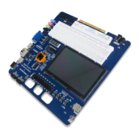
OLED
A Univision Technology Inc. UG-2832HSWEG04 is loaded on the DSDB. It is a white
monochrome, 128 × 32, 0.910-in. organic LED display matrix bundled with a Solomon Systech
SSD1306 display controller. The display data interface towards the Zynq programmable logic is
a 4-wire serial peripheral interface (SPI). The 4 wires in controller-terminology are CS#, D/C#,
SDIN, and SCLK, but CS# is hard-wired to ground. This adds to the reset and two power control
signals for proper start-up sequencing. The signals are summarized in Table 11.
 Loading...