NI Digital System Development Board User Manual | © National Instruments | 47
The +3V3 pin is driven by the 3V3_USER of the DSDB, and the +5V pin is driven by the
5V0_USER rail. See section Power Supplies for information on the characteristics of these
power rails.
DIO0-DIO15, UART.RX and UART.TX are connected to the programmable logic of the Zynq
via protection circuitry as described in section User IO Protection.
AO0 and AO1 are driven by a TI DAC7562SDSC 2-channel Digital to Analog converter. AO0
is connected to channel A of the DAC and AO1 is connected to channel B. The serial interface
of the DAC is connected to the programmable logic of the Zynq.
AI0-AI3 are connected to a TI ADS7950SBRGE 4-channel Analog to Digital Converter. AI0 is
connected to channel 0 of the ADC, AI1 is connected to channel 1, and so on. The serial interface
of the ADC is connected to the programmable logic of the Zynq.
For the Zynq pin assignments of DIO0-DIO15, UART.RX, UART.TX, the DAC serial bus and
the ADC serial bus see the Master XDC available on the DSDB Digilent Resource Center.
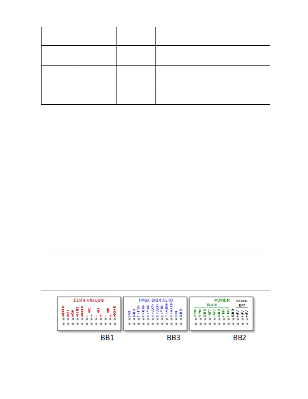
Breadboards
The DSDB board includes a large solderless prototyping area composed of 165 x 35mm
breadboard and 165 x 10 mm power strip, and three breadboards with signal connections that
give access to on-board signals and power supplies.
Figure 22. Signal Breadboards with Pinout
Each of the three signal breadboards has different functions described in the following sections.
UART.RX DGND Input UART receive input. UART lines are
electrically identical to DIO lines.
UART.TX DGND Output UART transmit output. UART lines are
electrically identical to DIO lines.
DGND N/A N/A Reference for digital signals, +5 V, and +3.3
V.
Table 27. MXP Pin Descriptions (Continued)
Signal
Name
Reference Direction Description
 Loading...