EasyManuals Logo
Home>Quectel>Control Unit>SC262R Series

Quectel SC262R Series User Manual

Quectel SC262R Series
127 pages
To Next Page IconTo Next Page
To Previous Page IconTo Previous Page
Page #50 background imageLoading...
Page #50 background image
Smart Module Series
SC200R&SC262R_Series_Hardware_Design 49 / 124
10 μF
EN
VIN
SW
NC
VOUT
VOUT
4
5
1
7
8
6
2
9
3
AGND
PGND
PGND
10K
22 μF/
10 V
1.0 μH
USB_DP
USB_DM
USB_VBUS
USB_ID
1
2
3
4
5
USB_DP
USB_DM
VUSB
USB_ID
GND
GND
GND
GND
GND
6
7 8
9
100 nF
Module
VBAT
GPIO
VBAT
C1
C2
L1
U1
R1
C3
D1 D2
D3
D4
ESDESDESD
ESD
GND
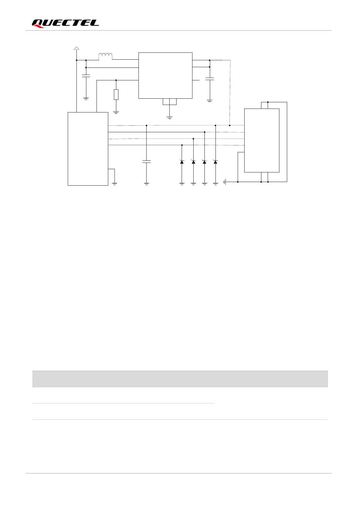
Figure 12: USB Interface Reference Design (OTG Supported)
In order to ensure USB performance, comply with the following principles when designing the USB
interface.
Route the USB signal traces as a differential pair with total grounding. The impedance of USB
differential trace should be controlled to 90 Ω.
Keep the ESD protection devices as close as possible to the USB connector. Pay attention to the
influence of junction capacitance of ESD protection devices on USB data lines. Typically, the
capacitance value should be less than 2 pF.
Do not route signal traces under crystals, oscillators, magnetic devices or RF signal traces. Route the
USB differential traces in inner-layer with ground shielding on not only the upper and lower layers but
also the right and left sides.
Make sure the trace length difference between USB 2.0 differential data signals is less than 0.7 mm.
Table 13: USB Trace Length Inside the Module
Pin No.
Signal
Length (mm)
Length Difference (DP - DM)
13
USB_DM
32.25
-0.10
14
USB_DP
32.15

Table of Contents

Questions and Answers:

Question and Answer IconNeed help?

Do you have a question about the Quectel SC262R Series and is the answer not in the manual?

Quectel SC262R Series Specifications

General IconGeneral
BrandQuectel
ModelSC262R Series
CategoryControl Unit
LanguageEnglish

Related product manuals