Smart Module Series
SC200R&SC262R_Series_Hardware_Design 89 / 124
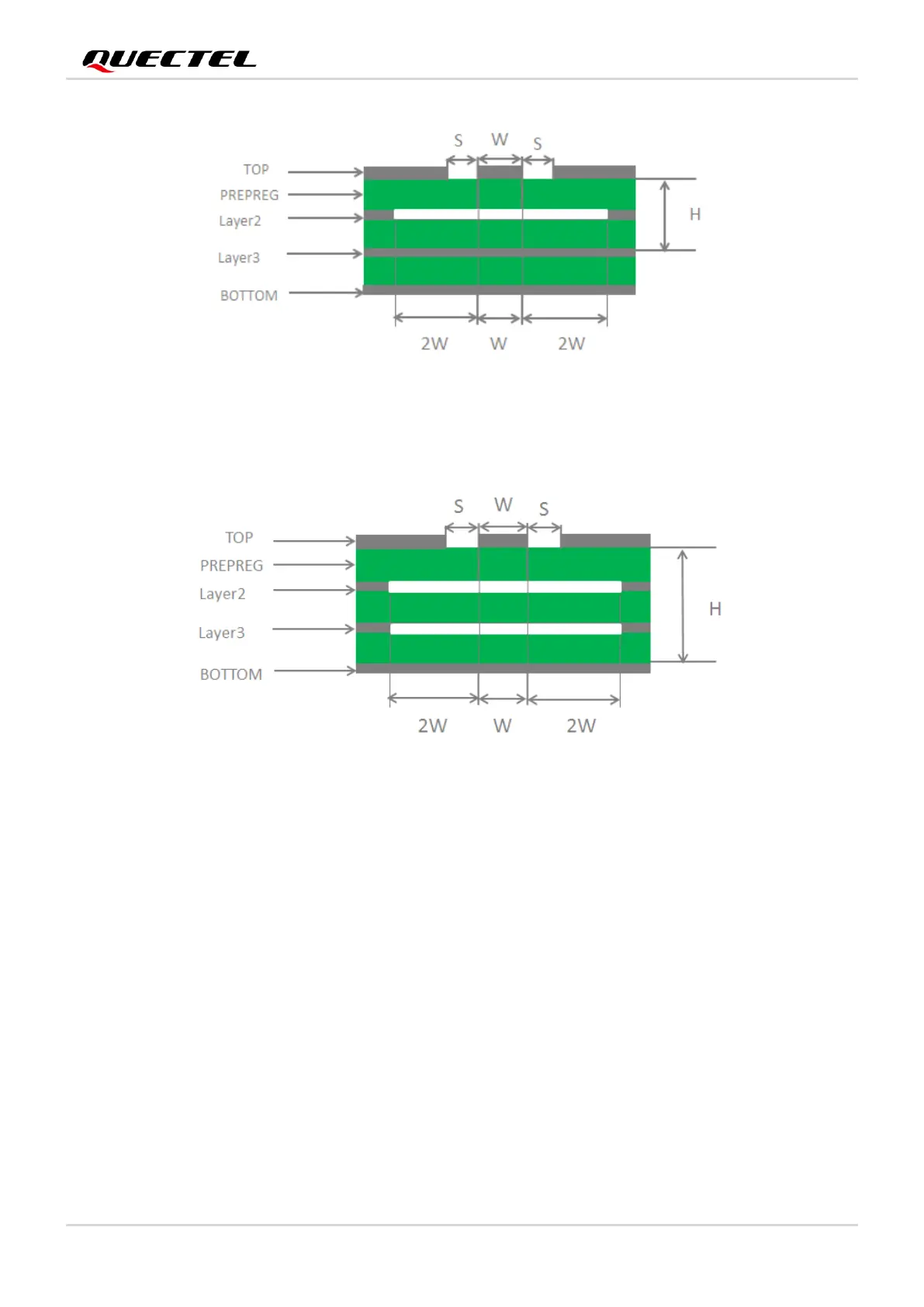
Figure 35: Coplanar Waveguide Design on a 4-layer PCB (Layer 3 as Reference Ground)
Figure 36: Coplanar Waveguide Design on a 4-layer PCB (Layer 4 as Reference Ground)
In order to ensure RF performance and reliability, follow the principles below in RF layout design:
⚫ Use an impedance simulation tool to accurately control the characteristic impedance of RF traces to
50 Ω.
⚫ Design the GND pins adjacent to RF pins as thermal relief pads, and fully connect them to ground.
⚫ Keep the distance between the RF pins and the RF connector as short as possible. Change all the
right-angle traces to curved ones and the recommended trace angle is 135°.
⚫ Reserve clearance under the signal pin of the antenna connector or solder joint.
⚫ Keep the reference ground of RF traces complete. Meanwhile, add some ground vias around RF
traces and the reference ground to improve RF performance. The distance between the ground vias
and RF traces should be no less than two times the width of RF signal traces (2 × W).
⚫ Keep RF traces away from interference sources, and avoid intersection and paralleling between
traces on adjacent layers.
For more details about RF layout, see document [3].
 Loading...