EasyManuals Logo
Home>Renesas>Computer Hardware>RL78/G13

Renesas RL78/G13 Application Note

Renesas RL78/G13
40 pages
To Next Page IconTo Next Page
To Previous Page IconTo Previous Page
Page #13 background imageLoading...
Page #13 background image
RL78/G13 Handshake-based SPI Master Transmission/Reception
R01AN6883EJ0100 Rev.1.00 Page 13 of 38
June.15.23
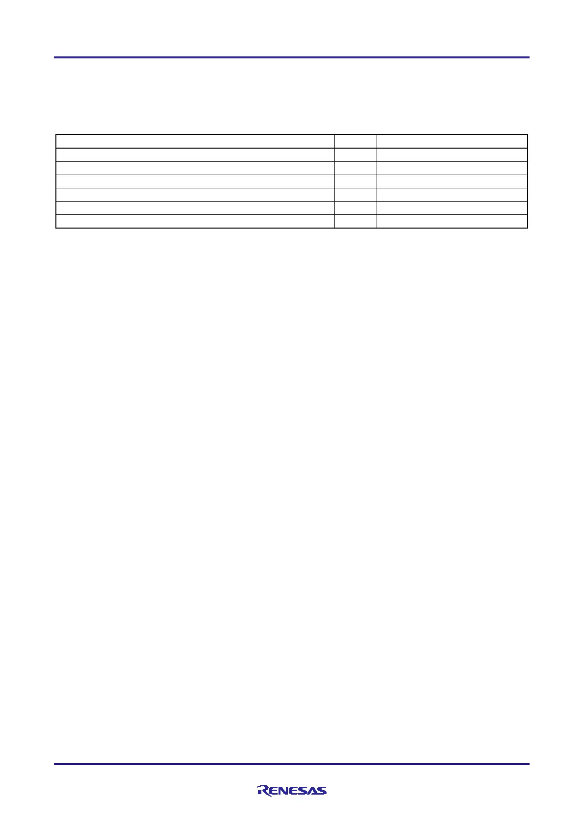
4.2 List of Pins to be Used
Table 4-1 lists the pins to be used and their functions
Table 4-1 Pins to be Used and Their Functions
Pin Name
I/O
Description
P10/SCK00/SCL00/(TI07)/(TO07)
Output
Serial clock output pin
P11/SI00/RxD0/ TOOLRxD/SDA00/ (TI06)/(TO06)
Input
Data reception pin
P12/SO00/TxD0/ TOOLTxD/(INTP5)/(TI05)/(TO05)
Output
Data transmission pin
P54
Input
BUSY signal input from slaves
P53/(INTP11)
Output
Slave 2 select signal
P52/(INTP10)
Output
Slave 1 select signal
Caution In this application note, only the used pins are processed. When actually designing your circuit,
make sure the design includes sufficient pin processing and meets electrical characteristic
requirements.

Other manuals for Renesas RL78/G13

Questions and Answers:

Question and Answer IconNeed help?

Do you have a question about the Renesas RL78/G13 and is the answer not in the manual?

Renesas RL78/G13 Specifications

General IconGeneral
BrandRenesas
ModelRL78/G13
CategoryComputer Hardware
LanguageEnglish

Related product manuals