- 18 -
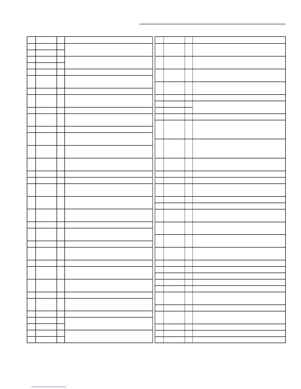
IC101 LA9241ML (Servo Signal Processor)
No. Pin Name I/O Function
1 FIN2 I Connection Pin for Photo Diode of Pickup.
2 FIN1 I FIN2 + FIN1 = RF, FIN2 - FIN1 = FE
3 E I Connection Pin for Photo Diode of Pickup.
4 F I E - F = TE
5 TB I Input Pin for DC ingredient of TE Signal.
6 TE- I Connection Pin for Gain Setting Resistor of TE
Signal to TE Signal Pin.
7 TE O Output Pin for Tracking Error Signal.
8 TESI I Input Pin for Track Error Sense Comparator.
TE Signal through Band Pass, and Inputted.
9 SCI I Input Pin for Shock Detection.
10 TH I Connection Pin for Time Constant Setting of
Tracking Gain.
11 TA O Output Pin for TA Amplifier.
12 TD- I Connection Pin for Constant Tracking Phase
Compensation, Consist of between TD and VR.
13 TD I Connection Pin for Constant of Tracking Phase
Compensation.
14 JP I Connection Pin for Amplitude Setting of Tracking
Jump (Kick Pulse) Signal.
15 TO O Output Pin for Tracking Control Signal.
16 FD O Output Pin for Focusing Control Signal.
17 FD- I Connection Pin for Constant of Focusing Phase
Compensation, Consist of between FD and FA.
18 FA+ I Connection Pin for Constant of Focusing Phase
Compensation, Consist of between FD- and FA-.
19 FA- I Connection Pin for Constant of Focusing Phase
Compensation, Consist of between FA and FE.
20 FE O Output Pin for Focusing Error Signal.
21 FE- I Connection Pin for Gain Setting Resistor of FE
Signal to FE Signal Pin.
22 AGND - Ground for Analog Signal.
23 SP O Output Pin for Single End of Input Signal of the
CV+, CV- Pin.
24 SPI I Input Pin for Spindle Amplifier.
25 SPG I Connection Pin for Gain Setting Resistor, when
Spindle 12 cm Mode.
26 SP- I Connection Pin for Constant of Spindle Phase
Compensation with SPD Pin.
27 SPD O Output Pin for Spindle Control Signal.
28 SLEQ I Connection Pin for Constant of Sled Phase
Compensation.
29 SLD O Output Pin for Sled Control Signal.
30 SL- I Input Pin for Sled Signal from Micro Processor.
31 SL+ I
32 JP- I Input Pin for Tracking Jump Signal from Digital
33 JP+ I Signal Processor.
No. Pin Name I/O Function
34 TGL I Input Pin for Tracking Gain Control Signal from
Digital Signal Processor. TGL = H : Gain Low
35 TOFF I Input Pin for Tracking Off Control Signal from Digital
Signal Processor. TOFF = H : OFF
36 TES O Output Pin for Track Error Sense Signal to Digital
Signal Processor.
37 HFL I High Frequency Level Signal Use Detection
Main-Beam Position is on the pit or mirror.
38 SLOF I Input Pin for Sled Servo Off Control.
39 CV- I Input Pin for Constant Linear Velocity Error
40 CV+ I Signal from Digital Signal Processor.
41 RFSM O Output Pin for RF Signal.
42 RFS- I Connection Pin for Gain Setting of RF and
Constant Setting of 3T Compensation of the
EFM Signal with RFSM Pin.
43 SLC O Slice Level Control Signal is Output Pin.
It Control Level of Data-Slice by Digital Signal
Processor of the RF Waveform.
44 SLI I Input Pin for Level Control of Data-Slice by
Digital Signal Processor.
45 DGND - Ground for Digital Signal.
46 FSC O Output Pin for Focus Search Smooth Condenser
47 TBC O Connection Pin for Variable Range Setting of
EF Balance.
48 NC - No Connect
49 DEF O Output Pin for Defect Detection of Disc.
50 CLK I Input Pin for Reference Clock Pulse.
(4.23 MHz of Digital Signal Processor)
51 CL I Input Pin of Clock Pulse for Command from
Micro Processor.
52 DAT I Input Pin of Data for Command from Micro
Processor.
53 CE I Input Pin of Chip Enable for Command from Micro
Processor.
54 DRF O Output Pin for Detect of RF Level.
55 FSS I Select Pin for Focus Search Mode
56 VCC2 - VCC for Servo and Digital Root.
57 REFI I Bus Control Connection Pin for Reference Voltage.
58 VR O Output Pin for Reference Voltage.
59 LF2 I Connection Pin for Time Constant Setting of
Detect Detection of the Disc.
60 PH1 I Capacitor Connection Pin for Peak-hold of RF Signal.
61 BH1 I Capacitor Connection Pin for Bottom-hold of
RF Signal.
62 LDD O Output Pin of APC (Automatic Power Control) Circuit.
63 LDS I Input Pin of APC (Automatic Power Control) Circuit.
64 VCC1 I VCC for RF Root.
IC BLOCK DIAGRAM & DESCRIPTION
 Loading...