 Loading...
Do you have a question about the Sony VPL-CX61 and is the answer not in the manual?
| Display diagonal | 0.79 \ |
|---|---|
| Lamp type | UHP |
| Lamp power | 190 W |
| Light source type | Lamp |
| Heat dissipation | 921.3 BTU/h |
| Projection technology | LCD |
| Contrast ratio (typical) | 350:1 |
| Projector native resolution | XGA (1024x768) |
| Dimensions (WxDxH) | 328 x 283.8 x 92.6 mm |
| Power requirements | AC 100 to 240 V, 50/60 Hz |
| Noise level | 28 dB |
| Power consumption (standby) | 5 W |
| Power consumption (typical) | 280 W |
| Storage temperature (T-T) | -20 - 60 °C |
| Operating temperature (T-T) | 0 - 35 °C |
| Storage relative humidity (H-H) | 10 - 90 % |
| Operating relative humidity (H-H) | 35 - 85 % |
| S-Video inputs quantity | 1 |
| VGA (D-Sub) ports quantity | 3 |
| Market positioning | Home cinema |
| Weight | 3700 g |
|---|
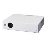
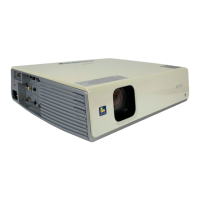
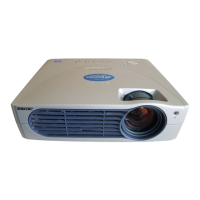
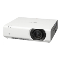
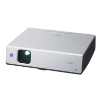
Shows the external appearance of the projector.
Identifies the locations of main circuit boards within the projector.
Procedure for removing the top cover of the projector.
Procedure for removing the QC board.
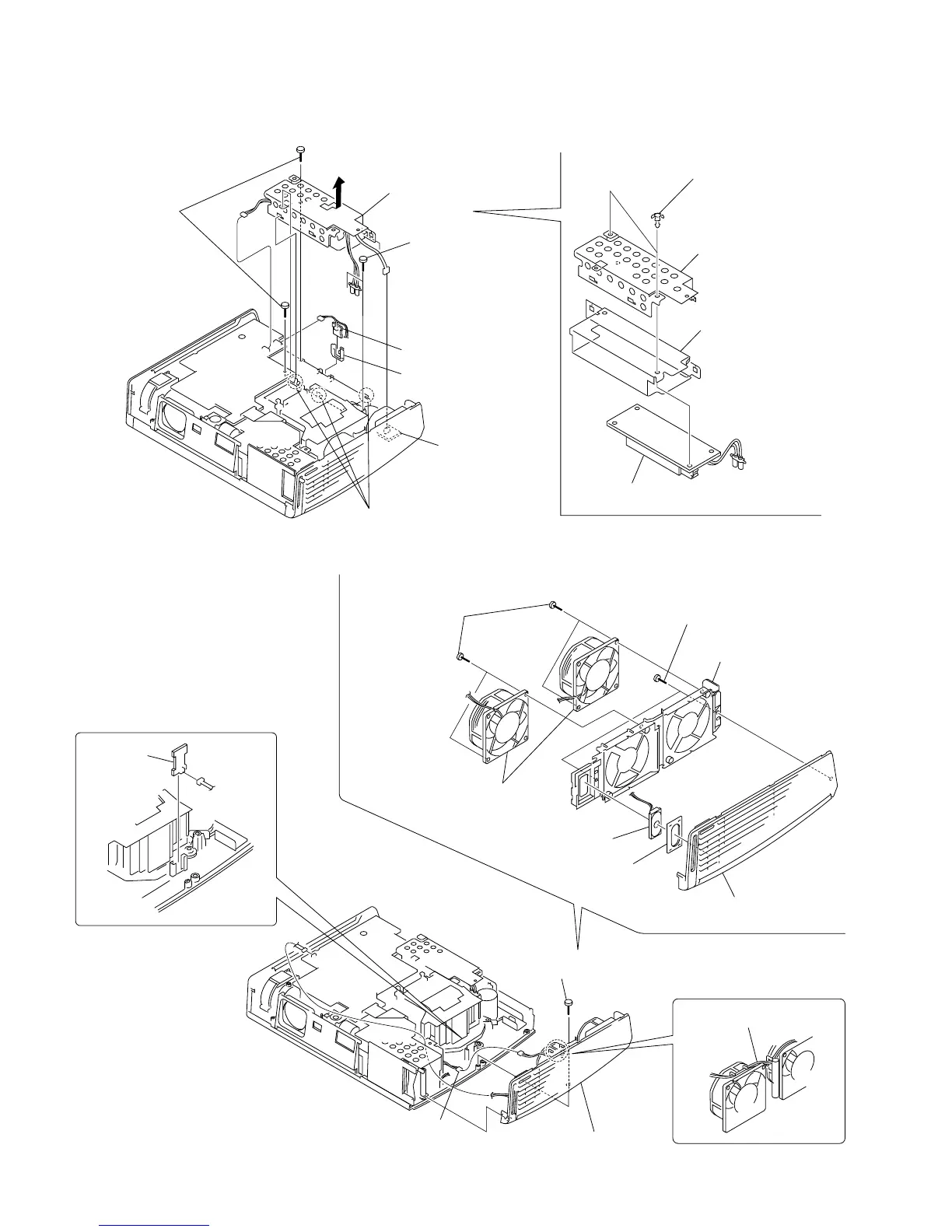
Procedure for removing the adjustor unit.
Procedure for removing the NR board and power supply block.
Procedure for removing the U board and speaker assembly.
Procedure for removing the GA board.
Procedure for removing the LH plate.
Procedure for removing the C board.
Procedure for removing the QA board.
Procedure for removing the optics block assembly.
Procedure for removing V, QC, and M boards.
Procedure for removing the GB board.
Procedure for removing the QB board.
Procedure for removing H2 board and side door.
Details the connection of C board extension with XC and XF32 boards.
Lists required equipment and steps to enter factory mode for adjustments.
Details the procedure for adjusting V COM values to minimize flicker.
Steps to follow after replacing the prism block, including adjustments.
Guidance on adjustments needed when replacing circuit boards.
Outlines preparation steps, including warm-up time and entering service mode.
Procedure for adjusting white balance in HIGH mode for INPUT-A.
Procedure for adjusting white balance in LOW mode for INPUT-A.
Procedure for adjusting white balance in HIGH mode for VIDEO input.
Procedure for adjusting white balance in LOW mode for VIDEO input.
Important notes regarding safety, standardization, stock, and units of repair parts.
Overall block diagram showing major functional units and their interconnections.
Detailed block diagram for C, QA, and QB boards.
Detailed block diagram for C board.
Detailed block diagram for C, H1, H2, L, NR, U, and V boards.
Detailed block diagram for C board.
Detailed block diagram for M and QC boards.
Detailed block diagram for GA and GB boards.
Schematic diagram for QA board, focusing on S-Video input.
Schematic diagram for QB board, covering RS-232C and Monitor Out functions.
Schematic diagram for QC board, detailing SIRCS receiver functionality.
Schematic diagram for C board, illustrating video/audio signal processing.
Schematic diagram for U board, showing lamp cover switch circuit.
Schematic diagram for V board, related to angle detection.
Schematic diagram for H1 board, covering panel switches and LEDs.
Schematic diagram for H2 board, covering panel switches and LEDs.
Schematic diagram for NR board, detailing SIRCS receiver functionality.
Schematic diagram for GA board, showing AC inlet and PFC control.
Schematic diagram for GB board, illustrating DC-DC converter circuit.
Board layout and schematic for QA board with S-Video input.
Board layout and schematic for QB board, covering RS-232C and Monitor Out.
Details methods and limits for measuring AC leakage current.