Table 5. JP1 configuration
Jumper Definition Setting Comment
JP1 Debugger selection
ON [1-2]
An external debugger connected to the
MIPI20 connector (CN5) can be used.
The level shifter (U1) is in high
impedance (high‑Z).
STLINK-V3EC no longer drives the
embedded STM32
OFF
The embedded STLINK-V3EC is
selected (default configuration).
Note:
The MIPI20 TRACE connector supports 1V8 or 3V3 for target reference voltage. When using the external debug
connector (CN5), STLINK-V3EC can be used to supply the board through the CN1 USB Type-C
®
connector.
Otherwise, another power supply source can be used as described in Section 8 Power supply.
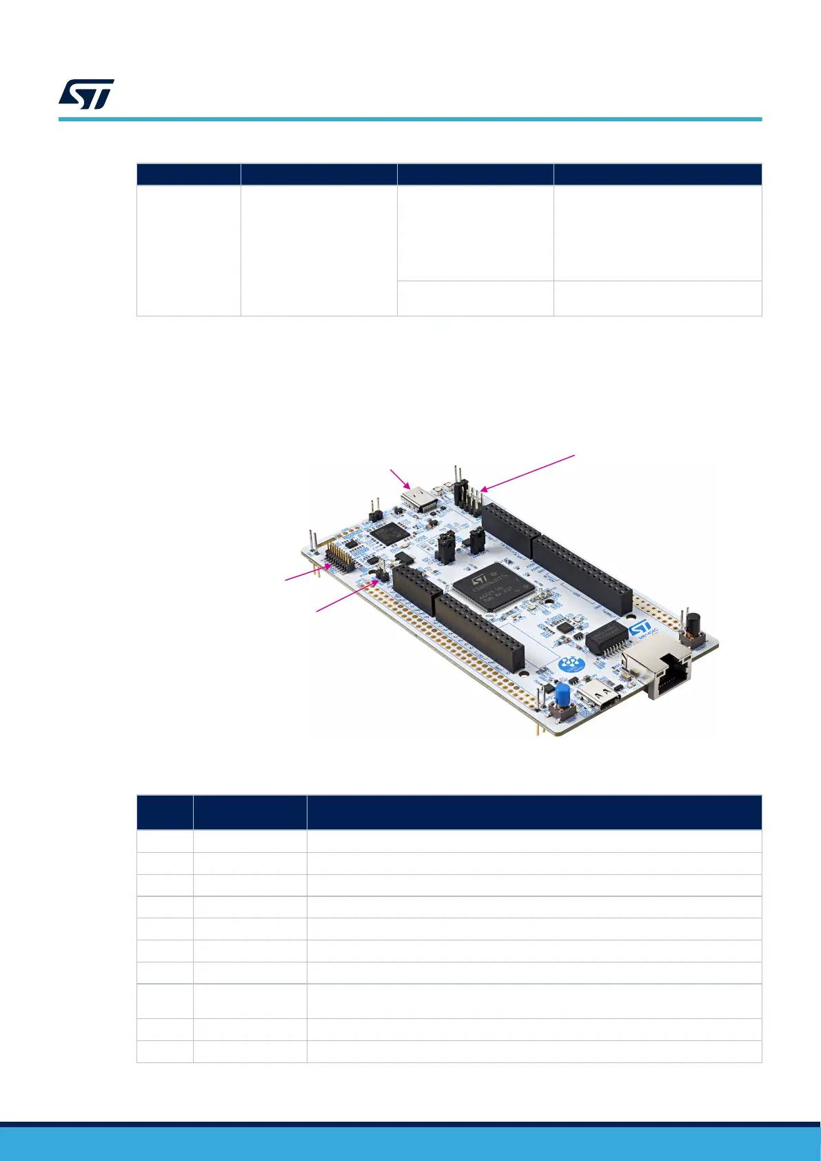
Figure 7. Connecting an external debug tool to program the on-board STM32
DT59063V1
5V power supply selection
(JP2)
STLINK-V3EC USB connector
(CN1)
MIPI20 connector
(SWD/JTAG/TRACE)
(CN5)
External debugger selection
(JP1)
Table 6. MIPI20 debug connector (CN5) pinout
MIPI20
pin
CN5 Designation
1 VTref Target reference voltage (fed from VDD)
2 SWDIO/JTMS Target SWDIO using SWD protocol or target JTMS using JTAG protocol
3 GND Ground
4 SWCLK/JCLK Target SWCLK using SWD protocol or target JCLK using JTAG protocol
5 GND Ground
6 JTDO/SWO Target SWO using SWD protocol or target JTDO using JTAG protocol
7 KEY Not connected
8 JTDI
Not used by SWD protocol, target JTDI (T_JTDI) using JTAG protocol, only for external
tools
9 GND Ground
10 NRST Target NRST using SWD protocol or target JTMS (T_JTMS) using JTAG protocol
UM3115
Embedded STLINK-V3EC
UM3115 - Rev 2
page 12/44

 Loading...


