NEO-8Q / NEO-M8 - Hardware Integration Manual
UBX-15029985 - R04 Production Information Hardware description
Page 8 of 31
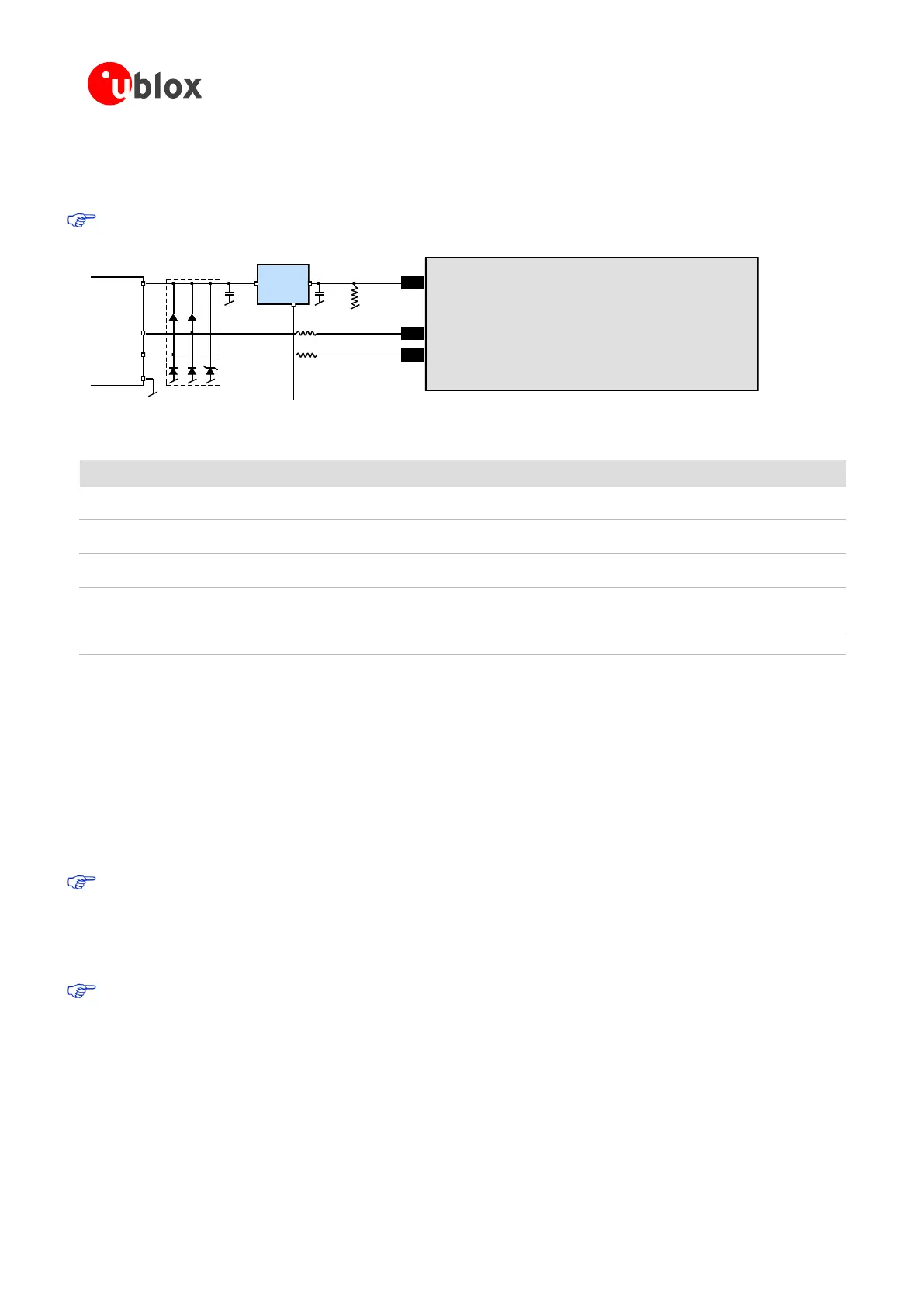
present and ready to communicate. This should be avoided by disabling the LDO (U1) using the enable signal
(EN) of the VCC-LDO or the output of a voltage supervisor. Depending on the characteristics of the LDO (U1) it is
recommended to add a pull-down resistor (R11) at its output to ensure VDD_USB is not floating if the LDO (U1)
is disabled or the USB cable is not connected i.e. VBUS is not supplied.
USB bus-powered mode is not supported.
Module
VDD_USB
LDO
VDD_USB
R4
USB_DP
USB_DM
R5
C24 C23
D2
VBUS
DP
DM
GND
USB Device Connector
U1
EN R11
EN
Figure 2: USB Interface
Regulates VBUS (4.4 …5.25 V)
down to a voltage of 3.3 V.
Almost no current requirement (~1 mA) if the GNSS receiver is operated as a
USB self-powered device.
Required according to the specification of LDO U1
Protect circuit from overvoltage
/ ESD when connecting.
Use low capacitance ESD protection such as ST Microelectronics USBLC6-2.
Serial
termination
resistors
Establish a full-speed driver
impedance of 28…44
A value of 27 is recommended.
100 k is recommended for USB self-powered setup.
Table 1: Summary of USB external components
1.4.3 Display Data Channel (DDC)
An I
2
C compatible Display Data Channel (DDC) interface is available on NEO-8Q and NEO-M8 series modules for
serial communication with an external host CPU. The interface only supports operation in slave mode (master
mode is not supported). The DDC protocol and electrical interface are fully compatible with the Fast-Mode of the
I
2
C industry standard. DDC pins SDA and SCL have internal pull-up resistors.
For more information about the DDC implementation, see the u-blox 8 / u-blox M8 Receiver Description
Including Protocol Specification [4]. For bandwidth information, see the corresponding product data sheet in the
Related documents. For timing parameters, consult the I
2
C-bus specification [7].
The NEO-8Q and NEO-M8 series DDC interface supports serial communication with most u-blox cellular
modules. See the specification of the applicable cellular module to confirm compatibility.
1.4.4 SPI
An SPI interface is available for communication to a host CPU.
SPI is not available in the default configuration, because its pins are shared with the UART and DDC
interfaces. The SPI interface can be enabled by connecting D_SEL to ground. For speed and clock
frequency, see the corresponding product data sheet in the Related documents.
1.4.5 TX_READY
The TX_READY function is used to indicate when the receiver has data to transmit. A listener can wait on the
TX_READY signal instead of polling the DDC or SPI interfaces. The UBX-CFG-PRT message lets you configure the
polarity and the number of bytes in the buffer before the TX READY signal goes active. The TX_READY function
can be mapped to TXD (PIO 06). The TX_READY function is disabled by default.
 Loading...